Most often, deliberation on PCB manufacturing takes center stage as a talking point. This is because of the continuous technological innovation and growth the industry experiences. The PCB helps to convey electronic elements within applications, thereby making growth possible
Many advancements and enhancements of PCB components are born. One of such enhancing components which are of great importance is the blind and buried vias. Via plays an incontestable role in the manufacturing process and design of the PCBs.
The inclusion of necessary PCB components in electronic gadgets nowadays is difficult. Thus, inventors congest more elements while maximizing the available space on the board.
The concept of the PCB vias is like a contortionist whose target is to maximize a fractional space.
Though, he uses his prerogative to decide the best way out of the available to meet the target. This is not visible in designing the PCB vias. There are various guiding principles to producing a very successful PCB design.
So, joining all the components and current paths on a single layer PCB may be difficult. Solution to this challenge is via. Vias are essential on the multilayer PCB, even though it is demanding to produce.
In a common two sided PCBs, via connects the surface level to the base level. It designs pathways for adequate movement of electrical current among the board and various layers. Drilling the PCB via using mechanization to produce electrical connections is worth noting.
Request Blind Buried Via PCB Quote, Pls Send PCB file to Sales@raypcb.com Now
Types of Via
There are different types of via, blind and buried vias are common. They allow compactness as well as reduce expansion difficulty. In a bid to maximize the capacity of Vias, an in-depth understanding of their variation is important. PCB design with vias and their advantages help in right decision making.
The VIA comprises two pads set up side by side on separate layers of the PCB design. The electrical channel becomes possible by the holes. Such hole in particular is copper plated which affirms its conductivity. It can also mean coated holes that allow electrical bonding within the layer.
A standard via contains a pad, a cylinder shape container (barrel) and an anti pad. Each via component has different functions. Anti pad is the space hole available connecting the barrel and foil layer. The pad links up the two ends of the cylindrical shape container with an electronic element. Furthermore, the barrel is the conductive passage for filling the hole.
Via is a big treasure in producing modern rigid multiplayer PCBs designs. Thus, the sizes of the PCBs are very small but are well loaded by cathode. Via has four various types i.e. Blind Via, through via, Buried Via and Stub via.
This article will focus its concentration on Blind via and buried via.
Blind vias PCB vs Buried vias PCB
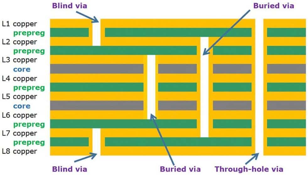
Blind and buried vias are a pair of choices available for linking surfaces and layers on the PCB. Generally, the distinction between the two types of PCB is that the Blind PCB via secures connection from the surface layer to either one or more internal layers, and it does not pass throughout the PCB.
Buried PCB via on the other side links two or more internal layers without piercing the outer layer. It might seem easy, yet various guiding regulations and restrictions control their use.
Furthermore, there are several restrictions to put in view before their use. Vias need a compulsory piercing of a flat number of coated layers. It does not begin from the base side of the hub nor can it stop at the top tier of it. Either blind or buried vias, they cannot stop inside or at the link of another via.
The most significant advantage both the blind and buried via gives to the PCB is the compacting of all elements on the design without adding an extra layer to the board. This option is great for managing space and meeting compact design conformism.
The use of the blind and buried via holes is a productive means to increasing solidity of a multilayer PCB. It reduces the PCB size and quantity of coated through holes. The buried and blind via structure are on all boot up managers’ boards.
The blind and buried vias has common features, these include:
- Increase in the integrity of the multilayer PCB, and the execution of its byproducts.
- The blind and buried vias gets rid of huge figures of through hole on the PCB
- They transform and mix up the inner link formation including the shape of the PCB design.
Blind Via PCB
The conventional process of designing PCBs shows meager via layout. It only allows through hole vias. Thus, adopting a drilling technique that manages depth will give room for extra via types.
The PCBs with blind vias keep to the customary process of designing PCBs up till the drilling stage. Addition of more holes for connection among two layers is necessary if the PCB has four layers.
Before the commencement of the PCB design, the need to decide on what buildup to adopt is vital. Inquiry from the PCB manufacturer is important as well. If consideration to add vias is on the go, repercussions might come up. The layout on the PCB will run out and in the end, the PCB might not be a good fit for use requesting a new design all together.
Furthermore, this will result in time wasting, efforts and money waste as well. To avoid these, there are some fundamental regulations blind via must observe.
Fundamental Regulations Blind Via PCB
The fundamental regulation blind via pcb must observe are as follows:
- The via must start from either the base or topmost surface of the PCB
- They have to occupy an even figure of layers.
- Their starting and ending point must not be at the middle of the PCB coating
- The via must not pass throughout the entire PCB
Remember that connections on the surface and inner layers of a multi layer PCB are part of the functions of the blind via. As a result, some restrictions and complications arise from drilling a blind via to a model depth.
In a bid to achieve a perfect coverage and metallic quality, the size of the via must be correct. As such, the hole depth to its diameter not exceeding 1 and 0.8 being the perfect value. Thus, gaping needs a bigger dimension. Big vias as well depicts that the insulator gap from the PCB layers is also great.
To prepare the blind vias, there is the need to drill via at the middle of the panel. Thereafter, the via passes through the layer ahead of other composite materials that assist in assembling the PCB layers
A point to note is between the route requirements and the processing capacity of the PCB, there must be a link. Thus, knowing the rules of designing a blind vias as laid down by the manufacturer will be profitable.
Request Blind Buried Via PCB Quote, Pls Send PCB file to Sales@raypcb.com Now
Buried Vias PCB
Identical to the blind via, the buried via as well provides linkage among layers. The layer count is in even figures like the blind via.
The difference between the blind and buried via is that the latter connects within the inner layer. Thus, there is no interjection between the internal and the external layer.
The buried vias is not visible from the surface area of the PCB. They are in the innermost layer of the PCB. Moreso, they need a different hole with coating.
The buried PCB design process is much the same as the blind PCB via. The only deviation being that the buried visa is out of sight to the surface layer. In developing a buried via PCB, the necessary mark out and pile up in the internal layer must be in place. Afterwards, develop and try out the vias.
The buried vias has the following advantages
- Wards off signal intrusion
- Lessens the PCBs aspect ratio
- Frees up regular space on the PCB
- Has the capacity to meeting the component restraints without an increase of the PCB size
Blind Vias
The blind vias are frequent in HDI PCBs. Its addition permits producers to enhance signal probity and PCB size reduction. This choice of blind vias brings a fresh routing option because big space is not needed for vias
Blind via form a linkage from the surface of the PCB to one or more internal layers without going through all the PCB. It is a viable option for high speed signal PCB. Blind vias have various manufacturing procedures, they include:
Photo defined blind vias
This type of process deals with overlaying a coat on light sensitive adhesive. The light reactive part is open which allows the superfluous materials to get stronger. The substances in the trench are taken out through engraving solutions. Copper covers both the trench’s external surface to create the surface layer of the PCB.
Laser drilled blind vias
This method is creating via by ray drilling of the copper and non conducting material in one phase. This comes after an overlay is on each of the PCBs sheets excluding the outer layer. It is very cheap and consumes less time.
Sequential lamination blind vias
In this procedure, a tiny piece of overlay goes through the manufacturing steps put to use in a double sided PCB. This includes drilling, engraving and plating after which the surface becomes covered. The method is expensive because of various manufacturing steps that need funding
Controlled depth blind vias
The method adopts a similar drilling process for through holes. Plating of the hole happens only when it gets to a particular depth in the PCB. Drilling is costly but this procedure is less expensive means to produce via.
Blind and Buried Vias in PCB
It is a general knowledge that a copper trace on a PCB is a transmitting path by which ends join on the board. A buried via joins at least two surfaces without interfering with exterior edges on the PCB. The blind via is a copper coated trench whose connection lies on a single outer layer of the PCB.
The trenches on the blind via do not cut the entire board whilst for the buried via, connection is in the circuit.
It is important to keep in mind that these vias are more for high viscous circuit panels. The ordinary boards do not need an extra diagram pattern because they are single layers.
The Blind Via in PCB
- Every hole own a single internal layer
- The size of the hole gives the distance between the surface and other similar internal layers.
- Drill file for trenches must be set out for blind vias. The measurement in depth for the trench must be lesser than or approximately one.
The Buried Via in PCB
- To avoid the risk of hitting other components in the PCB, the trench drill diameter in ratio must be less than 12
- Every hole must be on a distinct drill file even though the buried via connects various pieces in the layer
Blind Via Aspect Ratio
The blind via aspect ratio is an obscure issue so many producers neglect. Blind via aspect ratio is vital to different PCB applications. It is one of the factors that need consideration during the manufacturing process.
The blind via aspect ratio of a PCB plays a key role during the plating process. It explains the capacity of the synthetic process to protect copper coated trenches. The higher the aspect ratio, achieving dependable plating becomes tougher.
To understand the PCBs and its material demand, the density of the board should not be the only worry. Although, producers understand the acceptable standard for via aspect ratio of 8:1
The PCB via aspect ratio guides producers to ensure they conform to the device’s power. The Blind via aspect ratio is in length and height measurement. It is set by the width and trench diameter of the PCB
Via diameter serves as the parameter used during mechanical drilling to place via. This is because a little depth needs a tight drill. While a significant miss during trench drilling can render the PCB unfit for use.
Laser drilling expedites the shaping of small trenches without pressure on the panel. This procedure is a notable upgrade to the PCB manufacturing process.
Conclusion
By now, you have deep knowledge of the difference and similarities when comparing blind vias PCB vs buried vias PCB. If you have any more questions, feel free to contact us.
