The design of a Printed Circuit Board (PCB) antenna is a crucial aspect of any wireless communication system. The antenna’s performance can significantly affect the range, reliability, and data rates of the wireless system. The 915 MHz frequency band is a popular choice for industrial, scientific, and medical (ISM) applications, including remote monitoring, telemetry, and wireless sensor networks.
The PCB antenna design for the 915 MHz frequency band poses unique challenges due to the wavelength, board size, and material properties. The wavelength at 915 MHz is approximately 33 cm, which is much larger than the typical PCB size. Therefore, the antenna’s size must be optimized to fit the PCB while maintaining adequate performance. Additionally, the dielectric properties of the PCB material can affect the antenna’s impedance matching and radiation patterns. Therefore, careful consideration must be given to the PCB material selection and design.
In this article, we will discuss the key design considerations for a 915 MHz PCB antenna. We will explore the antenna’s size, shape, and ground plane design, as well as the impact of the PCB material on the antenna’s performance. We will also provide practical tips and guidelines for designing and optimizing a 915 MHz PCB antenna for your wireless communication system.
Antenna Basics
What is a PCB Antenna?
A PCB antenna, also known as a printed circuit board antenna, is an antenna that is printed onto a circuit board. It is a type of antenna that is commonly used in wireless communication systems. The main advantage of a PCB antenna is its low profile, which makes it ideal for use in compact devices such as smartphones, tablets, and wearables.
Why use a 915 MHz PCB Antenna?
A 915 MHz PCB antenna is designed to operate at a frequency of 915 MHz. This frequency is commonly used in industrial, scientific, and medical (ISM) applications, as well as in the Internet of Things (IoT) devices.
There are several reasons why a 915 MHz PCB antenna is a popular choice for these applications. First, it provides a good balance between range and power consumption. At this frequency, the antenna can transmit and receive signals over a relatively long distance while consuming minimal power. Second, it is compact and easy to integrate into a device. The antenna can be printed directly onto the circuit board, which eliminates the need for additional components and reduces the overall size of the device.
In summary, a 915 MHz PCB antenna is a popular choice for wireless communication systems that require a low-profile, compact, and energy-efficient antenna.
Design Considerations
When designing a 915 MHz PCB antenna, there are several considerations that must be taken into account. These include the frequency and wavelength, ground plane and feedline, radiation pattern, and gain.
Frequency and Wavelength
The frequency and wavelength of the antenna are important factors to consider in the design process. The wavelength of a 915 MHz signal is approximately 33 centimeters. This means that the antenna should be designed to be a quarter wavelength (8.25 cm) or a half wavelength (16.5 cm) in size.
Ground Plane and Feedline
The ground plane and feedline are crucial components of the antenna design. The ground plane should be large enough to provide a good ground plane for the antenna. The feedline should be designed to match the impedance of the antenna and the transmitter or receiver.
Radiation Pattern and Gain
The radiation pattern and gain of the antenna are also important considerations. The radiation pattern should be designed to provide a directional or omnidirectional signal, depending on the application. The gain of the antenna should be optimized for the desired range and signal strength.
In conclusion, designing a 915 MHz PCB antenna requires careful consideration of the frequency and wavelength, ground plane and feedline, radiation pattern, and gain. By taking these factors into account, it is possible to create an antenna that provides reliable and effective communication for a variety of applications.
Types of 915 MHz PCB Antennas

When it comes to designing a PCB antenna for 915 MHz applications, there are several types of antennas to choose from. The most common types of PCB antennas for 915 MHz applications are meandered monopole antennas, inverted-F antennas, and printed dipole antennas.
Meandered Monopole Antenna
The meandered monopole antenna is one of the most popular types of PCB antennas for 915 MHz applications. This type of antenna is relatively easy to design and can be printed on a single layer of PCB. Meandered monopole antennas are typically used in applications where a compact size is required.
Inverted-F Antenna
The inverted-F antenna is another type of PCB antenna that is commonly used for 915 MHz applications. This type of antenna is similar to the meandered monopole antenna, but it is inverted and has a ground plane. Inverted-F antennas are typically used in applications where a low profile is required.
Printed Dipole Antenna
The printed dipole antenna is a type of PCB antenna that is commonly used for 915 MHz applications. This type of antenna consists of two conductive elements that are printed on the PCB. Printed dipole antennas are typically used in applications where a high gain is required.
In conclusion, when it comes to designing a PCB antenna for 915 MHz applications, there are several types of antennas to choose from. The most common types of PCB antennas for 915 MHz applications are meandered monopole antennas, inverted-F antennas, and printed dipole antennas. Each type of antenna has its own advantages and disadvantages, and the choice of antenna will depend on the specific application requirements.
Simulation and Testing
Simulation Software
To ensure the effectiveness of the 915 MHz PCB antenna design, simulation software is utilized. This software allows for the creation of a virtual model of the antenna, which can then be tested and optimized before physical production. There are several simulation software options available, including CST Studio Suite, ANSYS HFSS, and Sonnet Suites.
CST Studio Suite is a popular choice for its user-friendly interface and advanced simulation capabilities. It allows for the creation of detailed models of the antenna and surrounding environment, including PCBs, components, and other structures. ANSYS HFSS is another widely used software, known for its accuracy and speed in simulating electromagnetic fields. Sonnet Suites is a specialized software that focuses on high-frequency electromagnetic analysis, making it an ideal choice for 915 MHz antenna design.
Testing Methods
Once the simulation process is complete, physical testing is necessary to verify the accuracy of the simulation results and ensure the antenna’s performance meets the desired specifications. There are several testing methods available, including far-field measurements, near-field measurements, and network analyzer measurements.
Far-field measurements are conducted in an open area, typically outdoors, and involve measuring the antenna’s radiation pattern and gain. Near-field measurements are conducted in a controlled environment, usually in a test chamber or anechoic chamber, and involve measuring the antenna’s electric and magnetic fields. Network analyzer measurements involve measuring the antenna’s impedance and return loss.
Overall, simulation and testing are crucial steps in the design process of a 915 MHz PCB antenna. By utilizing simulation software and testing methods, designers can optimize the antenna’s performance and ensure it meets the desired specifications.
Optimizing Performance
Tuning the Antenna
To achieve optimal performance from a 915 MHz PCB antenna, it is essential to tune the antenna to the desired frequency. This process involves adjusting the physical dimensions of the antenna elements to match the desired frequency. The tuning process can be done using a network analyzer or a spectrum analyzer.
To tune the antenna, start by adjusting the length of the antenna elements. The length of the elements determines the resonant frequency of the antenna. Keep adjusting the length until the desired resonant frequency is achieved. It is important to note that the resonant frequency of the antenna is affected by the dielectric constant of the PCB material being used.
Matching Network Design
Once the antenna is tuned to the desired frequency, the next step is to design a matching network. The matching network ensures that the antenna impedance is matched to the impedance of the transmitter or receiver. This is critical to ensure maximum power transfer and optimal performance.
The matching network can be designed using a Smith chart or a simulation tool such as ADS or CST. The matching network can be a simple L-match or a more complex circuit such as a pi-match or a T-match. The type of matching network used will depend on the impedance of the antenna and the transmitter or receiver.
In summary, optimizing the performance of a 915 MHz PCB antenna requires tuning the antenna to the desired frequency and designing a matching network to ensure maximum power transfer. With careful tuning and matching network design, it is possible to achieve excellent performance from a PCB antenna.
Manufacturing and Assembly

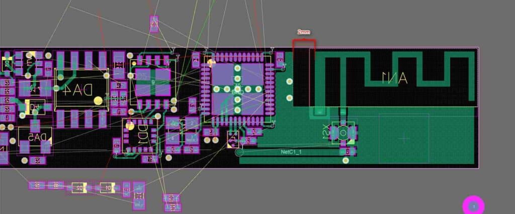
PCB Fabrication
The first step in manufacturing a 915 MHz PCB antenna is to fabricate the PCB. The PCB is designed using specialized software, and then the design is transferred to a manufacturer. The manufacturer uses a process called photolithography to etch the design onto a copper-clad board. The board is then drilled and plated to create the necessary connections.
It is important to choose a reliable PCB manufacturer with experience in fabricating high-frequency antennas. The thickness and quality of the copper layer, the spacing between traces, and the size of vias can all affect the performance of the antenna.
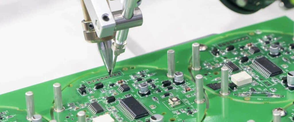
Assembly
Once the PCB is fabricated, the components can be assembled onto the board. The components used in the antenna design are surface-mount components, which can be placed on the board using automated pick-and-place machines.
It is important to follow the manufacturer’s recommended assembly process to avoid damaging the components or the PCB. The assembly process should also take into account any special requirements for the 915 MHz frequency band, such as the need for low-loss materials and careful placement of components.
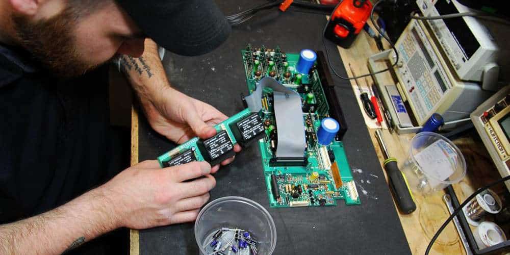
Soldering
The final step in the assembly process is soldering. Surface-mount components are typically soldered using reflow soldering, which involves heating the entire board to melt the solder and create a permanent connection.
It is important to use high-quality solder and to follow the recommended soldering profile to ensure that the components are properly soldered and that the antenna will perform as expected. In addition, any excess solder or flux should be carefully removed to avoid interfering with the performance of the antenna.
Overall, the manufacturing and assembly process for a 915 MHz PCB antenna requires careful attention to detail and a thorough understanding of the requirements for high-frequency antennas. By following best practices and working with experienced manufacturers and assemblers, it is possible to create a high-performance antenna that meets the needs of a wide range of applications.
Conclusion
In conclusion, designing a 915 MHz PCB antenna requires careful consideration of various factors such as the antenna type, size, and shape, as well as the surrounding environment and the intended application. By following the guidelines and principles outlined in this article, designers can create efficient and effective antennas that meet their specific requirements.
One of the key factors to keep in mind when designing a 915 MHz PCB antenna is the importance of matching the antenna impedance to the transmitter or receiver impedance. This can be achieved through various techniques such as using a matching network or adjusting the antenna dimensions. Another important consideration is the ground plane, which can significantly affect the antenna performance. By optimizing the ground plane size and shape, designers can improve the antenna efficiency and reduce unwanted radiation.
Furthermore, the choice of antenna type can also impact the overall performance and suitability of the design. For example, a monopole antenna may be more suitable for applications where space is limited, while a patch antenna may offer higher gain and directional radiation. Ultimately, the choice of antenna type will depend on the specific requirements and constraints of the application.
Overall, designing a 915 MHz PCB antenna requires careful attention to detail and a thorough understanding of the principles and techniques involved. By following the guidelines and best practices outlined in this article, designers can create high-performance antennas that meet their specific needs and requirements.
