Are you eager to learn about EMI PCB design? Are you also curious about the techniques required to reduce EMI in your PCB design and the challenges you may encounter? Have no anxiety! In this article, we’ll look at the stages for properly removing EMI in PCB design, the various techniques used to do this, the challenges you may face, the benefits of reducing EMI, and the future of EMI PCB design. We will also examine why we must adopt EMI-free PCBs daily. So, buckle up; it’s time to investigate the fascinating world of EMI PCB Design!
What is an EMI PCB design?
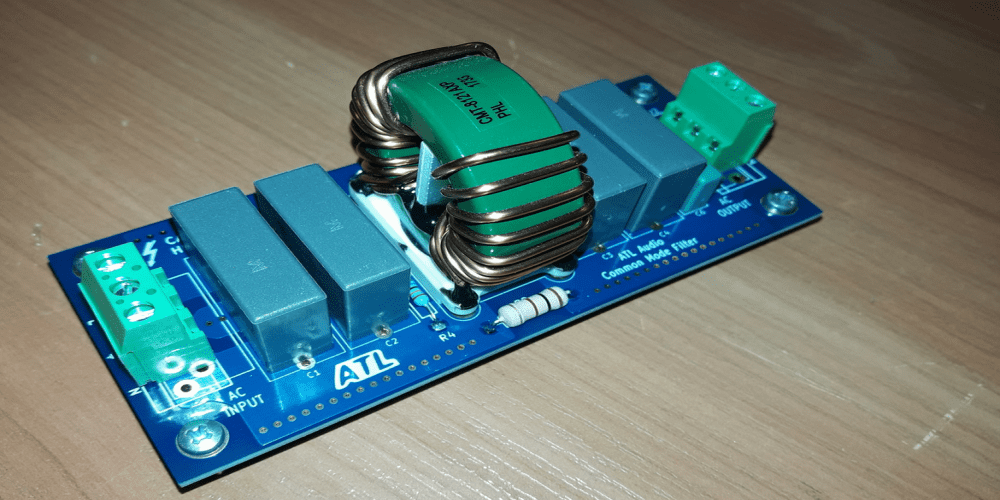
EMI PCB design is a printed circuit board (PCB) type that reduces the amount of electromagnetic interference (EMI) emitted by the device. This is easy to achieve by implementing several design techniques, such as increasing the distance between components, using unique EMI shielding materials, and adding ground and power planes. These techniques help to reduce the amount of noise emitted by the device, making it more reliable and compliant with applicable regulations.
Sources of EMI in PCB Design
There are many sources of electromagnetic interference. The following are some of these sources:
- Power lines:
Since the magnetic and electric fields produce high voltage or high current, power lines can produce EMI. This can be very hazardous if the power lines are adjacent to other delicate circuits on the PCB.
- Radio waves:
Radiofrequency (RF) transmissions can also produce electromagnetic interference (EMI), affecting other PCB circuits. It can be challenging to mitigate because RF waves are hard to restrict because they can pass through things like PCB and the air.
- Lightning:
Lightning can produce extraordinarily high levels of electromagnetic interference (EMI), harming electronic parts and interfering with delicate circuitry. This is a crucial factor to consider, in particular for outdoor electronic equipment.
- Internal sources:
Many PCB components, including switching regulators, oscillators, and digital signals, can produce EMI internally. These EMI sources can be particularly challenging to eliminate because they are already in the PCB design.
Steps to follow to Remove EMI in a PCB Design
Electromagnetic interference (EMI) removal in PCB (printed circuit board) design can be complex and need several stages. Some of the most important steps are as follows:
- Identify potential EMI sources:
The first step in eliminating EMI is to determine potential interference sources. This step entails looking at the circuit architecture and identifying elements like oscillators, switching regulators, and digital signals prone to producing EMI.
Optimize component placement:
Place components on the PCB to their best advantage. Shielding or filtering components help isolate sensitive circuits, or you may need to move elements around to reduce the space between them.
- Use proper grounding techniques:
Grounding is essential for reducing EMI. To lessen the possibility of EMI, you should use proper grounding techniques. This step entails employing a specialized ground plane to divide analog and digital signals or connecting many components to a single ground plane.
- Implement shielding and filtering:
In some circumstances, components for shielding or filtering help to eliminate EMI. While filtering components help remove undesired frequencies from signals, shielding can help prevent EMI from reaching sensitive circuits.
- Test and verify:
Following design optimization, you must ensure you have correctly eliminated EMI. This elimination may entail measuring the electromagnetic emissions from the PCB with an EMI analyzer or testing the PCB in real-world scenarios to ensure it functions as planned.
Testing EMI in PCB design
Do you need to test for EMI in your PCB design? If so, then the following details should help you maneuver around it. After that, you will have to follow the next steps:
- Define test criteria: Define frequency range, test method, and restrictions. Product standards should determine test criteria.
- Test equipment: Set up an EMI receiver, signal generator, spectrum analyzer, and oscilloscope. You should calibrate and validate before testing the equipment.
- Prepare the PCB: For testing, by connecting it to the test equipment, ensure that you properly install all components and power PCB correctly.
- Conduct radiated emission test: Conduct the radiated emission test by placing the PCB in an anechoic chamber and transmitting a signal with the signal generator while measuring the radiated emission level with the EMI receiver.
- Conduct conducted emission test: Conduct the conducted emission test by injecting a signal into the PCB’s power and signal lines while measuring the conducted emission level with the EMI receiver.
- Analyze the results: Analyze the test results to determine if the PCB design meets the test criteria. If the test results do not meet the criteria, identify the source of the emissions and take corrective actions such as adding EMI shielding or filtering.
Techniques to remove EMI in PCB design
There are many techniques for removing electromagnetic interference in your PCB design. The following are some of these techniques:

1. Trace Layout and Spacing:
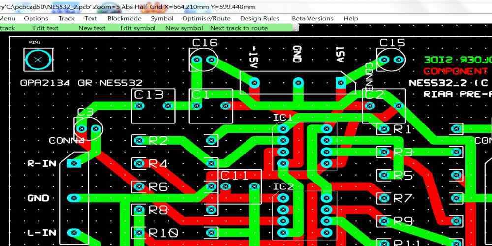
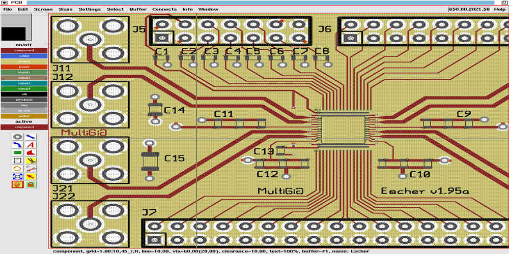
Regarding minimizing EMI, trace spacing and layout are two of the most crucial factors of PCB design. We should lay the traces, components, and other elements on the PCB to prevent interference and noise from one part from affecting the performance of another. You can achieve this by placing pieces to reduce the number of traces that cross one another and by widening the distance between trails that connect sensitive components. The trace spacing should be twice as wide as the actual trace. Additionally, you can reduce the amount of interference the trails produce by making the traces as short as feasible and eliminating sharp edges.
2. Using a ground plane:
A ground plane is a sizable copper region on the underside of a printed circuit board (PCB) that serves as a signal return path and offers a low-impedance connection to the ground. By serving as a shield that blocks the radiation of electric fields, ground planes help lower EMI. In addition, the ground plane connects to every digital component on the PCB, resulting in a more uniform current flow and decreased interference risk.
3. Shielding:
Designers can reduce EMI using metal enclosures or Faraday cages to shield sensitive components. The shields repel electromagnetic waves, keeping them from entering the board and interfering. Additionally, we can reduce the interference that reaches the PCB by using metal cables or wires with ferrite beads.
4. Positioning of PCB Layers:
The PCB’s layer configuration might reduce EMI. For example, you should use higher layers for traces carrying high-frequency signals, whereas for traces carrying low-frequency signals, you should use lower layers. Due to the higher layers’ greater susceptibility to interference, this design aids in reducing the amount of interference produced by the traces. Furthermore, engineers should position the ground plane as near as possible to the trails carrying high-frequency signals.
5. Dividing sensitive components:
Separating sensitive components from those that produce more noise is crucial for reducing the amount of interference between components. For instance, you should position analog components on the other side of the board from digital components. Additionally, you should separate high-frequency components from low-frequency components similarly.
6. Decoupling Capacitor:
Decoupling capacitors are tiny capacitors that help to reduce the amount of interference between components. Positioning these capacitors between the power source and the parts would be best to minimize noise production. Decoupling capacitors serve as a buffer, removing noise and keeping it from getting to the elements.
7. The Design of Controlled Impedance Transmission Lines:
Another efficient method to lower EMI is constructing transmission lines with regulated impedance. Designers can predetermine and change the impedance of controlled impedance traces according to the signal’s frequency. Since the impedance of the path matches the impedance of the signal, employing controlled impedance traces reduces the production of interference by traces. As a result, there are fewer reflections and noise-generating reflections.
Challenges Encountered in EMI removal in PCB design
Eliminating electromagnetic interference in a printed circuit board can be a daunting task. The following are the possible challenges you are likely to encounter:
1. Balancing form factor against board functionality and power:
EMI PCB design presents several challenges that require addressing to ensure the design meets performance, reliability, and regulatory requirements. Balancing form factors against board functionality and power is one of the most critical considerations in EMI PCB design. Designers must choose a form factor that is the most suitable for the application and power requirements while also ensuring that the board doesn’t exceed the maximum size dictated by size, weight, and power constraints.
2. Optimizing placement for best signal integrity/thermal performance:
Optimizing placement for best signal integrity and thermal performance is another critical challenge in EMI PCB design. Designers must consider the physical constraints of the board, such as the number of layers, routing paths, and component placement. Engineers must optimize placement to minimize crosstalk, ground bounce, and other signal integrity issues. It is also essential to optimize placement for thermal performance, ensuring that components are as close as possible to each other to minimize thermal resistance and maximize heat dissipation.
3. Keeping designs malleable:
Designers must also keep designs malleable enough to withstand assembly changes brought about by component shortages. As parts become more and more complex, component shortages become more common. Therefore, designers must create flexible designs to accommodate assembly changes to mitigate the risk of component shortages.
4. Managing trace lengths to minimize EMI radiation and interference:
Working trace lengths to reduce EMI radiation and interference is also crucial to EMI PCB design. Designers must consider the physical constraints of the board and use trace lengths that are as short as possible to reduce EMI radiation and interference. This is especially important in high-speed applications, where trace lengths must remain minimal.
5. Minimizing EMI generation:
Minimizing EMI generated by components on the board is another challenge in EMI PCB design. Power supplies, motors, and clocks can generate EMI, which must be minimized or eliminated. Designers must use EMI-compliant components and shielding, filtering, and other techniques to reduce EMI.
6. Ensuring that the board passes EMI compliance testing:
Ensuring the board passes EMI compliance testing is also essential in EMI PCB design. The board must pass tests for radiated and conducted emissions and susceptibility tests. In addition, designers must use appropriate PCB materials, components, and shielding to ensure that the board meets the necessary EMI compliance requirements.
7. Ensuring the board meets all regulatory requirements:
EMI PCB design must ensure that the board meets all relevant regulatory requirements. These requirements vary from country to country, and designers must research and understand the necessary regulations to ensure that their boards meet the requirements.
Effects of EMI on PCB design
Electromagnetic interference may often have some adverse effects on the functioning of a printed circuit board. The following are some of these effects:
1. Signal Integrity:
EMI’s most significant impact on PCB design is Signal Integrity problems. Electronic circuits might malfunction due to signal distortion from EMI. Data corruption, timing mistakes, and power supply noise can result from signal integrity issues. Designers should limit signal coupling on the PCB to reduce EMI’s influence on SI.
2. Radiant Emissions:
EMI in PCB design also causes radiated emissions. Radiated emissions are electromagnetic waves resulting from electronic devices. These waves can interfere with nearby electronic devices, causing interference or noise. To reduce the impact of radiated emissions, designers should use shielding and filtering techniques. Additionally, these waves can interfere with nearby electronic devices, generating noise. Shielding and filtering minimize radiated emissions.
3. Emissions Conducted:
Conducted emissions travel across the PCB’s power and signal lines. Emissions can cause noise or distortion in other electrical devices. Designers should ground the PCB and include filtering components to limit conducted emissions.
4. Crosstalk:
Crosstalk is the phenomenon in which the signals on different traces on the PCB interfere with each other. This interference may result in errors in the operation of electronic circuits. To mitigate the effects of crosstalk, designers should use techniques such as trace spacing, ground planes, and signal isolation.
5. Electromagnetic compatibility (EMC):
EMC is the ability of electronic devices to operate correctly in the presence of electromagnetic interference. EMC is essential for the proper functioning of electronic devices. The PCB design should consider the EMC requirements of the device and ensure that the device meets the EMC standards.
6. Heat Management:
EMI can affect PCB thermal management. When you expose electronic circuits to EMI, they generate heat. This heat can affect the performance of the courses and reduce their lifespan. To mitigate the effects of EMI on thermal management, designers should use proper cooling techniques such as heat sinks and fans.
Benefits of reducing EMI in PCB design
Despite the numerous challenges you may encounter while trying to reduce or eliminate electromagnetic interference, some benefits come with this process. Below are some of these advantages:
1. Enhancing Performance:
EMI can significantly impact electronic circuit performance, resulting in signal distortion, data loss, and mistakes. For instance, EMI produced by a PCB may interfere with other components, resulting in data loss, incorrect measurements, or even system failure. By eliminating EMI from PCB design, designers should ensure that electrical circuits operate more dependably, resulting in higher performance and stability.
2. Better Signal Integrity:
Signal corruption from EMI might result in mistakes or data loss. Therefore, to ensure the accurate transfer of signals and to enhance system performance, you should eliminate EMI from PCB design. This is crucial in analog or high-speed digital circuits where signal quality is paramount.
3. Increased Lifespan:
EMI may damage electronic components shortening their lifespan. For instance, if you expose a part to high levels of EMI for a long time, it may fail early and need replacement or repair. Therefore, designers should increase the lifespan of components and ensure that they will require less frequent replacement or maintenance by eliminating EMI from PCB design.
4. Regulatory Compliance:
Regulations limiting EMI emissions apply to several industries, including medical, automotive, and aerospace. For instance, the United States Federal Communications Commission (FCC) limits the amount of EMI that electronic equipment should generate. Designers may assist in ensuring that PCB designs adhere to these rules and prevent expensive fines or legal difficulties by eliminating EMI from PCB design.
5. Reduced Costs:
You can reduce electronic equipment production, testing, and maintenance costs by optimizing PCB design to eliminate EMI. For instance, a PCB that produces EMI could need extra shielding or filtering components to eliminate the interference. Designers can reduce the need for these additional components and save manufacturing costs by eliminating EMI from PCB design. In addition, lowering the likelihood of EMI-related component failure can help avoid needing pricey repairs or replacements.
6. Improved Safety:
EMI can interfere with critical systems, such as aerospace or medical applications. For instance, EMI produced by a PCB in a medical device may interfere with its operation and injure patients. Designers can contribute to ensuring that these systems function safely and dependably by eliminating EMI from PCB design.
7. Better User Experience:
Eliminating EMI from PCB design can enhance the user experience by lowering the possibility of interference or data loss. This feature can be particularly crucial in audio or video equipment applications, where EMI can cause considerable performance deterioration. For instance, a PCB help in a television that produces EMI may interfere with the video signal, resulting in a blurry image. By eliminating EMI from PCB design, designers may guarantee that the video signal moves accurately from point to point, improving picture quality.
The future of EMI PCB design
With the advent of new technologies and continued learning, we are likely to witness some changes in the field of PCBs. EMI is no exception. The following are some of the features to expect in the future:
· More sophisticated materials:
Designers anticipate creating more sophisticated materials that offer better EMI shielding capabilities. Researchers are looking at the possible applications of graphene in PCB design; for instance, they demonstrate good EMI shielding capabilities.
· Better simulation tools:
More sophisticated simulation tools will assist designers in seeing potential EMI problems before they arise. As a result, designers can more successfully optimize their designs for EMI as these tools advance.
· Increasingly intricate designs:
As electronic gadgets get more intricate and functional, the risk of EMI problems also rises. PCB designers must stay current with the newest technologies and methodologies to ensure their designs can manage these more complicated requirements.
· Greater emphasis on EMI compliance:
With regulating EMI emissions becoming more stringent, designers must exercise excellent care to ensure their designs adhere to the relevant requirements. Engaging in testing and certification services will probably be necessary more frequently to verify EMI compliance.
Applications of EMI-Free PCB Designs
Electromagnetic interference (EMI) is a common problem in electronic devices, and it can cause performance issues, data corruption, and even damage to the equipment. To mitigate this issue, engineers and designers use EMI-free PCB designs. These designs are essential for many industries, including consumer and wearable electronics, automotive, aerospace and defense, industrial manufacturing, and medical electronics. Let’s discuss the applications of EMI-free PCB designs in these industries:
Ø Consumer and Wearable Electronics
Wearable technology and consumer electronics are essential to our everyday lives. These gadgets are user-friendly, portable, and trim. However, they also produce a sizable quantity of electromagnetic interference, which can harm nearby devices. In this sector, it’s essential to have EMI-free PCB designs to guarantee that the devices work without disturbance. Additionally, these designs assist makers in meeting legal requirements and lower the possibility of product recalls due to safety issues.
Ø Automotive
In the automotive industry, the likelihood that electromagnetic interference will lead to issues has increased with the use of electronic devices in vehicles. The seamless operation of automotive electronics without interference from other systems or devices is easily achievable with EMI-free PCB designs. Furthermore, these EMI-free designs also increase car safety due to the potential for accidents caused by malfunctioning electronic systems.
Ø Defence and Aerospace
Electronic systems are crucial to the operation of aircraft, satellites, and other equipment in the aerospace and defense sectors. These systems must endure challenging environments to avoid interfering with other devices or systems. EMI-free PCB designs are essential in this sector for these systems to continue operating without disruption because even slight interference can have disastrous effects.
Ø Industrial Production
EMI-free PCB designs are also crucial in industrial production. A substantial amount of electromagnetic interference comes from manufacturing machines and equipment, which can be problematic for nearby machines and equipment. The smooth operation of these machines’ electrical systems without interference from other systems or devices requires EMI-free PCB designs. These designs also increase worker safety by lowering the possibility of device failure or mishaps.
Ø Medical Electronics
EMI-free PCB designs are essential in medical technology, as well. Medical systems or other electronic devices nearby may experience issues due to the electromagnetic disturbance that electronic medical devices produce. These devices work without disrupting other systems or equipment thanks to EMI-free PCB designs. These designs also increase patient protection by lowering the possibility of equipment failure or inaccurate readings.
Conclusion
In conclusion, designing EMI PCBs is an intricate process that demands a thorough analysis of the design approaches and EMI mitigation options. Using the right design strategies and materials, designers can reduce EMI and ensure the device complies with the required EMI conformance standards. As new technologies develop, more sophisticated simulation tools and materials ought to become accessible as well, assisting creators in better optimizing their designs for EMI. EMI-free designs are necessary to ensure the security and dependability of many sectors because they have many advantages. Therefore, integrate EMI-free PCB designs into your designs to advance your product. Also, let’s work together to ensure that our electrical devices are dependable and secure and that our PCB designs are EMI-free.
