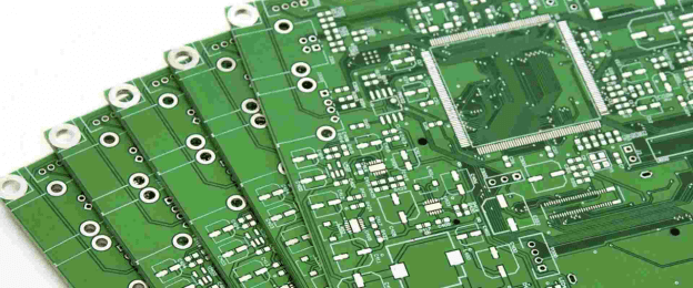
The majority of electronics use printed circuit boards (PCBs) as the foundation for physically supporting and wiring the surface-mounted and socketed components.
A bigger-scale version of the photolithographic method used to create conductive routes in processors is used to create PCBs for applications, like in computers that require precise conductive traces.
Composition
A PCB resembles a layer of cake in certain ways. Heat and glue are used to laminate together alternating layers of different materials to create a single PCB product.
A finished PCB with solder dabs in place is normally assembled with electronic components by a machine. An industrial oven is used to bake the PCB and melt the solder that connects the parts. Most PCBs are comprised of copper traces and fiberglass or glass-reinforced polymers. They also have a soldermask layer.
The soldermask layer is the one that is placed on top of the copper foil. The PCB’s green hue stems from this layer.
The mask is applied to the copper circuit so that the copper traces are protected from coming into accidental touch with other solder, metals, or conductive bits. This is accomplished by covering the copper circuit with the mask. This layer protects against solder jumps and enables the user to solder in the correct positions during the process.
Following the soldermask layer, the white silkscreen layer is applied. With the addition of letters, numbers, and symbols on the silkscreen, the PCB can be assembled more quickly and has descriptors that make the board easier for people to comprehend.
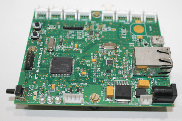
For straightforward electronic devices, PCBs can be single-layer. There can be up to twelve layers on printed circuit boards for sophisticated gear, like motherboards and graphics cards.
PCB board printing is only a momentary step in the production of PCBs that enables you to print your own circuit boards. Typically their manufacture starts with designing the PCB to suit the function of their creation.
Then comes the executive production of the circuit boards, which involves the printing of the boards. However, there are still some post-production steps of printed circuits like PCB assembly of components.
Before we take a look at printing PCBs, it is only fitting that a proper understanding of PCBs is established. There are various types and varying complexities of printed circuit boards.
Types of Printed Circuit Board
Overview
Based on the manufacturing procedures, design criteria, and application requirements, such as those for medicine, automobile, defense, and space industries, printed circuit boards (PCBs) are divided into numerous categories.
Different sorts of PCB boards can now be produced thanks to more intricate designs that are based on consumer requests and specifications. Before choosing a PCB, you should look at a few factors such as the amount of space needed, how stress is handled, and the PCB’s mechanical and electrical stability. Available PCBs include:
Single-Sided PCBs
The most typical sort of printed circuit board is a single-sided PCB. Above the substrate, it has a solitary copper route on the surface that conducts electricity. On one side of the board, where the electrical components are soldered or positioned, the fully etched circuit is visible.
Because there is only one conducting layer on these boards, the conductive channels are quite large and cannot intersect or overlap.
These PCBs are therefore appropriate for low-density design requirements. FM radios, timing circuits, power supplies, LED lighting boards, and other basic and inexpensive electrical/electronic devices all use a single-sided printed circuit board.
They are affordable, simple to produce, appropriate for low-density designs, simple to repair, and simple to design.
Double-Sided PCBs
On both the top and bottom sides of this PCB, a small layer of conductive material, such as copper, has been applied. You can electrically connect through-hole components from one side to the other via drill holes in the circuit board.
Through-hole technology or surface mount technology are two mounting techniques used by these PCBs to link the circuitry on each side. With through-hole technology, lead components are inserted into the circuit board’s drill holes and then soldered to pads on the opposing sides.
Electrical components must be precisely positioned on the circuit boards’ surface to use surface mount technology.
Cell phone systems, power monitoring, test equipment, amplifiers, HVAC applications, UPS systems, and many other applications employ double-sided PCBs.
Multi-Layer PCBs
There are more than two copper layers on multilayer PCBs. In general, this category includes any board with at least three conducting layers. In the sandwich architecture of multilayer PCBs, there are several conductive layers that are on both sides of the board. These conductive layers are separated by an equal number of sheets of insulating material.
Ensure that there are no air gaps and that the finished PCB assembly is appropriately stable, all of these must be fused and laminated together at high pressures and temperatures.
Tech gadgets, GPS trackers, medical equipment, and several other more complicated circuits and gadgets employ multilayer PCBs.
Rigid PCBs
This type of circuit board is firm and cannot be bent or folded. A hard substrate serves as the board’s foundation, giving it strength and rigidity. They consist of several layers, such as a silkscreen layer, copper layer, solder mask layer, and substrate layer, which are joined by glue and heat.
Rigid PCBs can be single-sided, double-sided, or multi-layered, but some circuit boards are only one of these depending on the application. But once they’re made, they can’t be altered or changed.
Rigid PCBs are utilized in a variety of products, including temperature sensors, control tower instrumentation, GPS equipment, computers, laptops, tablets, and mobile phones.
Flexible PCBs
The various printed circuits and components that make up a flexible printed circuit board are organized on a flexible substrate. A transparent conductive polyester sheet, polyether ether ketone, or polyamide is frequently used to create flexible PCBs.
Similar elements as those being used to make rigid printed circuit boards are employed to build these printed circuit boards. The board’s ability to conform to the desired form during operation is the main distinction.
These PCBs come in single-sided, double-sided, and multilayer variations. As a result, the unit assembly’s complexity is decreased.
Flex PCBs are utilized in the production of organic light emitting diodes (OLEDs), LCDs, flex solar cells, the automotive industry, cellular phones, cameras, and sophisticated electronics goods including laptop computers.
Tools & Materials
The material and tools for printing a circuit board can vary greatly depending on the type of etching for the PCB production. Yet, regardless of whether etching be mechanically done, machine assisted, or done via the use of an etching solution, there’s a general list of items that one can use and they include
- PC and printer
- Transparent slides
- Indian ink
- Cotton buds
- Paper towel
- UV light source
- Photo-sensitive PCB boards
- NaOH
- Sodium persulfate
- 2 Plastic or glass containers
- Rubber gloves to protect your hands
- A photo frame
- Drillbits
- 2 empty 1L bottles
- Copper Boards
- Laser printer
- Fine sandpaper or Kitchen Scrubber
- Hydrochloric Acid
- Hydrogen Peroxide
- Thinner or Acetone
- Plastic container
- Circuit diagram
- Electronic or Hand Driller
- Hacksaw
- Etching solution
Making Your Circuit Board Design
Select a technique for building the PCB. The materials required by the process, its level of technical difficulty, or the type of PCB you want to get will typically determine your option. Here is a summary of the various techniques and their key advantages:
- Acid etching method: this procedure is somewhat slow, necessitates the use of various materials, including the etchant, and calls for considerable safety precautions. Depending on the materials you use, the quality of the PCB you get will vary, but generally speaking, it is a decent method for circuits with low to medium degrees of complexity. Alternative techniques are typically used in circuits with smaller wires and closer wiring.
- UV etching method: This procedure, which is utilized to transfer your PCB layout onto your PCB board, calls for more expensive materials, some of which may not be widely accessible. However, the procedures are very straightforward and can result in finer and more intricate circuit architectures.
- Routing method: To use this technique, specialized equipment is needed that can mechanically scrape away extra copper from the board or run empty separators between wires. If you want to purchase one of those pieces of equipment, it can be pricey, and typically renting one requires access to a nearby workshop. However, this technique works well if you need to duplicate the circuit frequently and manufacture high-quality PCBs.
- Laser etching method: Large production businesses typically use this, however certain institutions may also have it. Although the idea is similar to mechanical etching, the board is etched using LASER beams. Such computers are typically difficult to obtain, but if perhaps your local university is one of the fortunate ones to have one, you are welcome to use their resources if they permit.
The next thing is to make your circuit’s PCB layout. You must sketch the circuits using an etchant-resistant substance for acid etching.
If you want to sketch by hand, special markers can be easily acquired for this purpose. This is not appropriate for medium to large circuits. However, the material most frequently utilized is ink for laser printers.
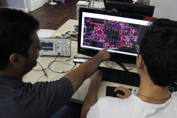
This is often accomplished by using PCB layout software to transform the schematic design of your circuit into a PCB layout. There are various open-source programs available for designing and creating PCB layouts.
Printing Your PCB Layout
Once you are satisfied with the schematic of the PCB design on your computer, you should match the size of the design in the software to the circuit board and the paper to ensure that they are the proper sizes.
The File menu of the software can be used to print the diagram. On glossy paper, like magazine paper, print it out. Before doing that, you should make sure the circuit is mirrored.
Most PCB design layout programs have this as an option when printing. After printing, be careful not to touch the ink-covered portion of the paper because it could get on your hands.
Ironing the Printed PCB Layout
Align the circuit board and the paper circuit diagram. The diagram should be facing the copper part of the circuit board. Around this time your iron should be on. Wait for the iron to heat up after setting it to the cotton setting.
The iron should be heated before being gently placed on top of the paper covering the circuit board. The iron should be left there for 30 to 45 seconds.
Afterward, lift the iron, carefully set it aside, and carry the circuit board to the nearest water source. Do not pull the paper off the circuit board; it should be attached to the board.
Hold the circuit board beneath the water as it begins to flow. Start slowly removing the paper, and it should soon all fall off. You might attempt soaking a little bit longer if some sections look very challenging to pull off.
You should have a copper board with your PCB pads and signal traces etched out in black toner if everything went according to plan.
Board drying. Simply letting the large water droplets drip out or gently wiping them off with a napkin or sponge can remove them. It shouldn’t take more than 30 seconds, and you shouldn’t rub the circuit vigorously because that could cause the ink to peel off.

Etching the PCB Board
Use acid to etch the board. By doing this, the etching solution removes any unwanted copper thickness from the board, leaving only the wiring for the final circuit. Pick an etching acid. Ferric chloride is a typical etchant option. Crystals of ammonium persulfate or other chemical solutions can be used, though.
Other etching methods, specifically the mechanical and Laser printer methods, use machines and laser beams to etch the board, and are more suitable for complex circuits.
Get the acid etchant ready. There may be extra instructions, depending on the acid etch you select. For instance, certain crystalline acids must be dissolved in hot water, whilst other etchants can be used immediately.
Immerse the board in the acid. Be mindful to stir the mix every three to five minutes. Once all extra copper has been etched off the board, remove it and wash it.
Eliminate the used insulating drawing substance. For practically all types of insulating drawing materials used in PCB layout drawings, specialized solvents are readily accessible. However, you may use fine sandpaper if you don’t have access to any of these things.
Conclusion
It is that simple to design and print a PCB from scratch, with a computer program and a few materials. This fact has greatly contributed to the ease of research in electrical and electronics engineering.
