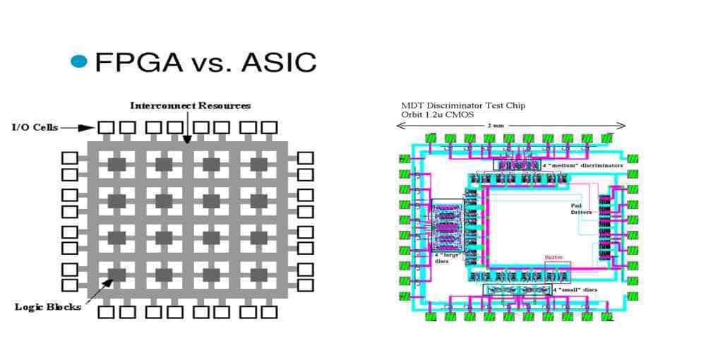
FPGA (Field-Programmable Gate Array) is a type of integrated circuit that can be programmed by the user to perform specific functions. The design of an FPGA PCB layout is crucial for the performance and reliability of the device. FPGA PCB layout involves the placement and routing of the components on the board to minimize noise, crosstalk, and other interference.
The design of an FPGA PCB layout requires a deep understanding of the FPGA architecture and the specific requirements of the application. The layout must take into account factors such as power supply, clock distribution, signal integrity, and thermal management. The goal is to create a design that meets the performance requirements while minimizing the cost and complexity of the board.

Basics of FPGA PCB Layout
FPGA (Field Programmable Gate Array) is an integrated circuit that can be programmed after manufacturing. FPGA PCB (Printed Circuit Board) layout is the process of designing a PCB for an FPGA-based system. The goal is to ensure that the FPGA functions optimally and reliably. Here are some basics of FPGA PCB layout:
Component Placement
Component placement is critical in FPGA PCB layout. The FPGA should be placed close to the power supply and decoupling capacitors. The power supply should be placed on the PCB’s edge for easy access. The FPGA should be placed away from noisy components such as switching regulators. The oscillator should be placed close to the FPGA to reduce jitter.
Power and Ground Planes
FPGA PCB layout should have separate power and ground planes. The power plane should be thick enough to handle the FPGA’s power requirements. The ground plane should be connected to the FPGA’s ground pins and all other ground points. The power and ground planes should be placed close to each other to minimize the inductance and resistance.
Signal Integrity
Signal integrity is a crucial factor in FPGA PCB layout. The signals should be routed carefully to avoid crosstalk and noise. The high-speed signals should be routed using controlled impedance traces. The differential signals should be routed as closely as possible to each other. The vias should be placed away from the signal traces to avoid reflections.
Thermal Management
FPGA PCB layout should have proper thermal management. The FPGA generates heat, and it should be dissipated efficiently. The PCB should have thermal vias to transfer heat to the ground plane. The FPGA should be placed in a location with good airflow. The PCB should have a heat sink or a fan to cool the FPGA.
Conclusion
FPGA PCB layout is a complex process that requires careful planning and execution. The basics of FPGA PCB layout include component placement, power and ground planes, signal integrity, and thermal management. By following these guidelines, you can design a reliable and high-performance FPGA-based system.
Design Considerations for FPGA PCB Layout

When designing a PCB layout for an FPGA, there are several key considerations to keep in mind. Here are some of the most important factors to consider:
Component Placement
The placement of components on the PCB is critical to the performance of the FPGA. It is important to place the FPGA as close as possible to the power supply and decoupling capacitors, as well as any other critical components. Additionally, it is important to keep the traces between the FPGA and other components as short as possible to minimize signal degradation.
Power Supply
The power supply for the FPGA must be carefully designed to ensure that it is stable and free from noise. This can be achieved by using a low-dropout regulator (LDO) or a switching regulator, depending on the specific requirements of the design. Additionally, it is important to place decoupling capacitors as close as possible to the FPGA to filter out any noise on the power supply.
Signal Integrity
Signal integrity is critical to the performance of the FPGA. It is important to keep the signal traces as short as possible to minimize signal degradation, and to ensure that all traces are properly terminated to prevent signal reflections. Additionally, it is important to ensure that the impedance of the traces matches the impedance of the FPGA to prevent signal distortion.
Thermal Management
FPGAs can generate a significant amount of heat, which can affect their performance and reliability. It is important to carefully design the PCB to ensure that the FPGA is properly cooled. This can be achieved by using heat sinks, thermal vias, or other cooling techniques.
EMI/EMC
FPGAs can generate electromagnetic interference (EMI), which can affect other components on the PCB. It is important to design the PCB to minimize EMI by using proper grounding techniques, shielding, and filtering.
In summary, when designing a PCB layout for an FPGA, it is important to consider component placement, power supply design, signal integrity, thermal management, and EMI/EMC. By carefully considering these factors, it is possible to design a PCB layout that maximizes the performance and reliability of the FPGA.
Best Practices for FPGA PCB Layout
When designing a PCB layout for an FPGA, it’s important to follow certain best practices to ensure optimal performance and reliability. Here are a few key tips to keep in mind:
-
Keep high-speed signals as short as possible: High-speed signals, such as clock and data lines, should be kept as short as possible to minimize signal degradation and ensure consistent signal timing. Use high-quality signal routing techniques, such as differential pairs, to reduce noise and crosstalk.
-
Minimize the number of vias: Vias can introduce signal reflections and increase signal delay, so it’s important to minimize their use whenever possible. Use blind and buried vias to reduce the number of vias needed and avoid using vias in high-speed signal paths.
-
Ensure proper power and ground distribution: A well-designed power and ground distribution system is critical to ensuring optimal FPGA performance. Use multiple power and ground planes to reduce noise and ensure adequate current capacity. Place decoupling capacitors as close to the FPGA as possible to minimize noise and voltage fluctuations.
-
Follow manufacturer guidelines: Always refer to the manufacturer’s guidelines and datasheets when designing an FPGA PCB layout. These documents provide important information on signal timing, power requirements, and other critical design considerations.
-
Use simulation and analysis tools: Simulation and analysis tools, such as SPICE and IBIS models, can help identify potential signal integrity issues and optimize PCB layout designs. Use these tools to evaluate signal timing, crosstalk, and other key performance metrics.
By following these best practices, you can design a high-performance and reliable PCB layout for your FPGA-based system.
Tools and Resources for FPGA PCB Layout
Designing a PCB layout for an FPGA can be a challenging task, but with the right tools and resources, it can be made much easier. Here are some of the most useful tools and resources for FPGA PCB layout:
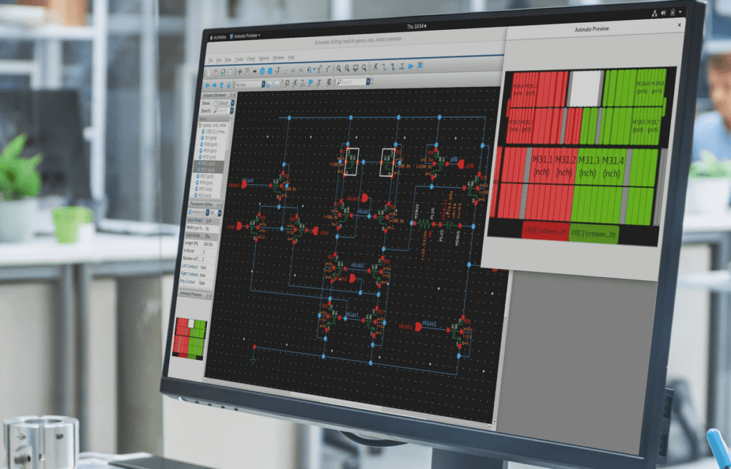
PCB Design Software
PCB design software is an essential tool for FPGA PCB layout. There are many different options available, but some of the most popular include Altium Designer, Eagle PCB, and KiCAD. These tools offer a range of features to help with FPGA PCB layout, including schematic capture, component placement, and routing.
FPGA Development Kits
FPGA development kits are another useful resource for FPGA PCB layout. These kits typically come with a pre-designed PCB layout that can be used as a starting point for your own design. They also often include reference designs and application notes that can help with the layout process.
Online Resources
There are many online resources available for FPGA PCB layout. Websites such as the Xilinx PCB Design Hub and the Altera PCB Design Resource Center offer a wealth of information and resources to help with FPGA PCB layout. These resources include design guidelines, application notes, and reference designs.
Design Rule Check (DRC) Tools
Design rule check (DRC) tools are essential for ensuring that your PCB layout meets the requirements of your FPGA. These tools check your design against a set of rules to ensure that it is manufacturable and meets the requirements of your FPGA. Examples of DRC tools include Altium Designer’s DRC tool and the DRC tool included with KiCAD.
Signal Integrity Simulation Tools
Signal integrity simulation tools are also important for FPGA PCB layout. These tools allow you to simulate the behavior of your design and ensure that it meets the signal integrity requirements of your FPGA. Examples of signal integrity simulation tools include HyperLynx SI and Altium Designer’s Signal Integrity tool.
In conclusion, there are many useful tools and resources available for FPGA PCB layout. By using these tools and resources, you can make the process of designing a PCB layout for an FPGA much easier and more efficient.
