Table of Contents
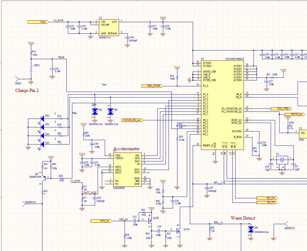
ToggleFrom schematic to PCB is a crucial step in the process of electronic design. The schematic is the blueprint of the circuit, and the PCB is the physical manifestation of that design. The transition from schematic to PCB is where the design becomes a tangible reality.
The process of going from schematic to PCB involves several steps. First, the schematic must be converted into a netlist, which is a list of all the connections between components. This netlist is then imported into PCB design software, which allows the designer to lay out the physical components and traces that will make up the circuit. Once the layout is complete, the software generates the necessary files to manufacture the PCB, including the Gerber files that specify the exact dimensions and placement of each component.
Designing a PCB can be a complex and challenging task, but it is a critical step in the process of creating electronic devices. From the initial schematic to the final product, every step along the way requires careful attention to detail and a deep understanding of the principles of electronic design. With the right tools and knowledge, however, anyone can take their ideas from the drawing board to the real world.

Creating a Schematic
Selecting Components
When creating a schematic, the first step is to select the components that will be used in the circuit. This involves considering the specifications and requirements of the circuit, such as voltage and current ratings, as well as the physical constraints of the PCB.
It is important to choose components from reputable manufacturers and suppliers, and to ensure that they are available in the required quantities and at a reasonable cost. Some common components used in electronic circuits include resistors, capacitors, diodes, transistors, and integrated circuits.
Placing Components
Once the components have been selected, they must be placed on the schematic in the appropriate locations. This involves considering the overall layout of the circuit and the physical constraints of the PCB.
Components should be placed in a logical and organized manner, with related components grouped together and arranged in a way that minimizes the length of the connections between them. It is also important to ensure that there is adequate space between components to allow for routing of the PCB.
Connecting Components
The final step in creating a schematic is to connect the components together using wires or other connections. This involves considering the electrical requirements of the circuit, such as the need for ground connections and the direction of current flow.
Connections should be made in a clear and organized manner, with wires routed in a way that minimizes the length and complexity of the connections. It is also important to ensure that connections are properly labeled and documented to facilitate future troubleshooting and maintenance.
Overall, creating a schematic is an important step in the design of a PCB, and requires careful consideration of the components, layout, and connections of the circuit.
Designing the PCB Layout

Importing the Schematic
Before starting the PCB layout design, importing the schematic is the first step. The schematic design is the blueprint of the circuit that shows how all the components are connected. It is essential to ensure that the schematic is error-free and complete before importing it into the PCB design software.
Most PCB design software allows for easy importing of schematics. The software automatically creates a netlist that contains all the connections between the components. The netlist is used to guide the software in placing the components on the PCB.
Placing Components on the PCB
After importing the schematic, the next step is to place the components on the PCB. The placement of the components is crucial for the performance of the circuit. The designer needs to consider factors such as signal integrity, thermal management, and ease of assembly.
The PCB design software provides tools for placing components on the board. The designer can drag and drop components onto the board and adjust their position manually. The software also provides an auto-placement feature that can be used to speed up the process.
Routing the Traces
Once the components are placed on the PCB, the next step is to route the traces. The traces connect the components and carry the signals between them. The designer needs to ensure that the traces are routed in a way that minimizes signal interference and noise.
The PCB design software provides tools for routing the traces. The designer can manually route the traces using the software’s routing tools. The software also provides an auto-routing feature that can be used to speed up the process.
In conclusion, designing the PCB layout is a critical step in the PCB design process. The designer needs to ensure that the schematic is error-free and complete before importing it into the PCB design software. The placement of the components is crucial for the performance of the circuit, and the traces need to be routed in a way that minimizes signal interference and noise.
Generating Gerber Files

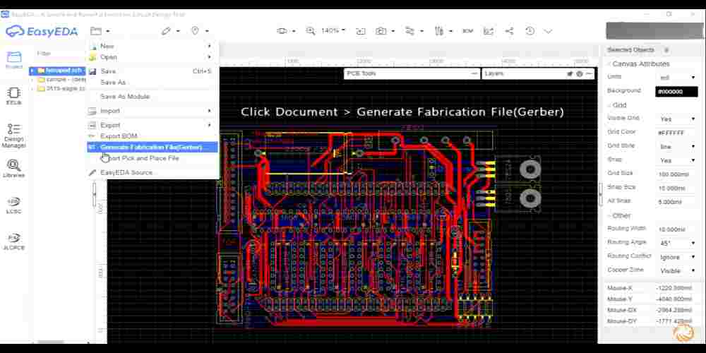
Once the schematic and layout of the PCB are completed, the next step is to generate Gerber files. Gerber files are a standard format used in the PCB manufacturing industry to convey the design information to the manufacturer.
To generate Gerber files, the PCB design software has a built-in option to export the files. The exported files usually include the following:
- Top and bottom copper layers
- Top and bottom silkscreen layers
- Top and bottom solder mask layers
- Drill files for the holes
- Board outline
It is important to double-check the exported files to ensure that they are correct and complete. Any missing or incorrect files can cause manufacturing errors.
Gerber files can be generated in different formats such as RS-274X or RS-274D. The RS-274X format is the newer format and includes more information such as aperture definitions, which are used to control the size and shape of the copper traces.
Before sending the Gerber files to the manufacturer, it is recommended to use a Gerber viewer to check the files. The viewer can display the files in a 2D image, which makes it easier to check for errors such as missing traces or overlapping pads.
In conclusion, generating Gerber files is a crucial step in the PCB manufacturing process. It is important to ensure that the files are correct and complete before sending them to the manufacturer. Using a Gerber viewer can help to avoid any errors that could cause manufacturing issues.

