Full bridge rectifiers are an essential component in many electronic circuits. They are used to convert AC voltage into DC voltage, which is necessary for many different applications. The PCB layout of a full bridge rectifier is critical to its performance and efficiency.
The layout of a full bridge rectifier PCB must take into account several factors, including the size and placement of the components, the routing of the traces, and the thermal management of the circuit. The size and placement of the components are important because they affect the overall size of the PCB and the ease of assembly. The routing of the traces is critical because it affects the impedance of the circuit and the noise performance. The thermal management of the circuit is important because it affects the reliability and performance of the rectifier over time.

Basic Layout Considerations
When designing a full bridge rectifier PCB layout, there are a few basic considerations that must be taken into account to ensure optimal performance. These include component placement, trace routing, grounding, and decoupling.
Component Placement
Component placement is critical to the success of any PCB design. When placing components for a full bridge rectifier, it is important to consider the following:
- Keep the high voltage components away from low voltage components to prevent noise and interference.
- Place the diodes as close to the transformer as possible to reduce noise and voltage spikes.
- Keep the output capacitors close to the diodes to minimize inductance and reduce ripple voltage.
Trace Routing
Trace routing is the process of connecting components on a PCB with copper traces. When routing traces for a full bridge rectifier, it is important to consider the following:
- Use wide traces to reduce resistance and minimize voltage drop.
- Keep the traces as short as possible to minimize inductance and reduce noise.
- Route the traces away from high voltage components to prevent noise and interference.
Grounding
Grounding is an important consideration in any PCB design. When grounding a full bridge rectifier, it is important to consider the following:
- Use a star grounding scheme to minimize noise and interference.
- Connect the ground plane to the chassis to reduce noise and improve safety.
- Keep the ground plane as large as possible to reduce impedance and improve performance.
Decoupling
Decoupling is the process of adding capacitors to a PCB to filter out noise and improve performance. When decoupling a full bridge rectifier, it is important to consider the following:
- Place decoupling capacitors as close to the power pins of the integrated circuits as possible to reduce noise.
- Use multiple capacitors in parallel to reduce inductance and increase capacitance.
- Use ceramic capacitors for high frequency decoupling and electrolytic capacitors for low frequency decoupling.
By considering these basic layout considerations, you can ensure that your full bridge rectifier PCB layout is optimized for performance and reliability.
Full Bridge Rectifier Circuit

A full bridge rectifier circuit is a type of rectifier circuit that is commonly used in power supply applications. It is a four-diode circuit that converts alternating current (AC) into direct current (DC). The circuit is called a “full bridge” because it uses four diodes arranged in a bridge configuration.
Circuit Diagram
The circuit diagram for a full bridge rectifier is shown below:
As shown in the diagram, the AC input is applied to the two ends of the bridge. The output is taken from the two remaining ends of the bridge. The four diodes are arranged in a bridge configuration, and each diode conducts during one half-cycle of the AC input.
Component Selection
The components used in a full bridge rectifier circuit are critical to its performance. The diodes used in the circuit should be rated for the maximum voltage and current that will be encountered. The transformer used to step down the AC voltage should have a center-tapped secondary winding.
The output filter capacitor used in the circuit should be chosen based on the output voltage and current requirements. The capacitor should be rated for the maximum voltage and current that will be encountered, and its capacitance should be chosen to provide adequate filtering of the output voltage.
In conclusion, a full bridge rectifier circuit is a simple and effective way to convert AC to DC. By carefully selecting the components used in the circuit, it is possible to achieve high efficiency and low ripple in the output voltage.
PCB Design Guidelines
Layer Stackup
The layer stackup of a full bridge rectifier PCB is an important consideration for the design. A four-layer stackup is typically used, with the power and ground planes on the inner layers. This helps to reduce the length of the signal traces and minimize noise. The outer layers are used for routing signals and power to the components. It is important to ensure that the layer stackup is balanced to avoid warping of the PCB during manufacturing.
Trace Width and Spacing
The trace width and spacing are important parameters to consider when designing a full bridge rectifier PCB. The trace width should be selected based on the current rating of the circuit. A wider trace width is required for higher current ratings to minimize resistance and heat generation. The spacing between traces should also be carefully selected to avoid crosstalk and interference.
Via Placement
The placement of vias is an important consideration in the design of a full bridge rectifier PCB. Vias should be placed in a way that minimizes the length of the signal path and reduces the risk of interference. It is also important to ensure that the vias are properly connected to the ground plane to minimize noise.
Silkscreen and Labeling
Silkscreen and labeling are important for the assembly and maintenance of the full bridge rectifier PCB. The silkscreen should be used to indicate the component locations and polarity. The labeling should be clear and legible to ensure that the circuit can be easily identified and maintained.
In conclusion, following these PCB design guidelines can help to ensure the reliable and efficient operation of a full bridge rectifier circuit.
Thermal Considerations

Heat Sinks
When designing a full bridge rectifier PCB layout, thermal considerations are of utmost importance. The high currents involved in rectification can generate a lot of heat, which can damage the components if not dissipated properly. One way to dissipate heat is to use heat sinks. Heat sinks are designed to absorb heat from a component and then dissipate it into the surrounding air. They are typically made of aluminum or copper, which have high thermal conductivity.
When selecting a heat sink for your full bridge rectifier, it is important to consider the size and shape of the heat sink. The size of the heat sink will depend on the amount of heat that needs to be dissipated and the thermal resistance of the heat sink. The shape of the heat sink will depend on the available space on the PCB and the orientation of the components.
Thermal Relief Pads
Another way to dissipate heat in a full bridge rectifier PCB layout is to use thermal relief pads. Thermal relief pads are copper pads that are connected to the ground plane of the PCB. They are designed to reduce the thermal resistance between the component and the PCB, which allows heat to be dissipated more efficiently.
When designing a full bridge rectifier PCB layout, it is important to use thermal relief pads for components that generate a lot of heat. The size and shape of the thermal relief pads will depend on the size and shape of the component and the amount of heat that needs to be dissipated.
In conclusion, when designing a full bridge rectifier PCB layout, it is important to consider the thermal considerations. Heat sinks and thermal relief pads are two ways to dissipate heat and protect the components from damage. By carefully selecting the size and shape of these components, you can ensure that your full bridge rectifier operates efficiently and reliably.
Testing and Troubleshooting
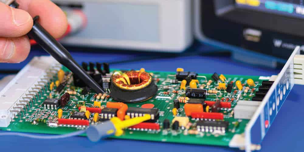
Testing Procedure
After designing and assembling the full bridge rectifier PCB, it is essential to test it to ensure it is working correctly. The following testing procedure can be done to verify the functionality of the PCB:
- Connect the input AC voltage to the PCB and measure the output DC voltage using a multimeter.
- Verify the output voltage is the expected value, which is the input voltage minus the voltage drop across the rectifier diodes.
- Check for any abnormal heating on the PCB, which may indicate a short circuit or overcurrent.
- Verify the ripple voltage is within the acceptable range by measuring the AC voltage component of the output signal.
Common Issues and Solutions
Despite careful design and assembly, full bridge rectifier PCBs may encounter issues during testing. Here are some common issues and solutions:
- No output voltage: Check for any open circuit connections on the PCB, verify the input voltage, and check the diodes’ polarity.
- Low output voltage: Verify the input voltage and check for any voltage drops on the PCB, such as resistive losses or diode voltage drops.
- High ripple voltage: Verify the input voltage and check for any capacitive or inductive coupling between the input and output signals. Increase the value of the output filter capacitor to reduce the ripple voltage.
- PCB overheating: Check for any short circuits on the PCB, verify the input voltage, and reduce the load current if necessary.
In conclusion, testing and troubleshooting are essential steps in ensuring a full bridge rectifier PCB’s proper functionality. By following the testing procedure and identifying common issues and solutions, any potential problems can be resolved promptly.
