Gates are fundamental building blocks in digital logic design. They are electronic circuits that perform logical operations on one or more binary inputs to produce a single binary output. Gates are used to create more complex circuits and are essential in the design of digital systems such as computers, calculators, and mobile devices.
There are several types of gates, including AND, OR, NOT, NAND, NOR, and XOR gates. Each gate has a unique truth table that defines the output for each possible combination of inputs. For example, an AND gate outputs a 1 only when both its inputs are 1, while an OR gate outputs a 1 when either of its inputs is 1. Gates can be combined to create more complex circuits that perform more sophisticated operations.
Understanding gates is essential for anyone interested in digital logic design. By learning how gates work and how they can be combined to create more complex circuits, designers can create efficient and effective digital systems that meet the needs of their users. In this article, we will explore the basics of gates, their functions, and how they can be used to create more complex circuits.

Basic Gates
In digital logic design, gates are the fundamental building blocks that are used to create complex digital circuits. Gates are electronic devices that perform logical operations on one or more binary inputs and produce a single binary output. There are several types of basic gates, which include:
NOT Gate
The NOT gate is the simplest type of gate, also known as an inverter. It has only one input and one output. The output of the NOT gate is the opposite of the input. If the input is 0, the output is 1, and vice versa. The NOT gate is represented by the symbol ‘¬’ or ‘!’ in digital logic.
AND Gate
The AND gate has two or more inputs and one output. The output of the AND gate is 1 only if all the inputs are 1. Otherwise, the output is 0. The AND gate is represented by the symbol ‘∧’ in digital logic.
OR Gate
The OR gate also has two or more inputs and one output. The output of the OR gate is 1 if any of the inputs are 1. If all the inputs are 0, the output is 0. The OR gate is represented by the symbol ‘∨’ in digital logic.
NAND Gate
The NAND gate is a combination of the AND gate and the NOT gate. It has two or more inputs and one output. The output of the NAND gate is the opposite of the AND gate output. If all the inputs are 1, the output is 0. Otherwise, the output is 1. The NAND gate is represented by the symbol ‘⊼’ in digital logic.
NOR Gate
The NOR gate is a combination of the OR gate and the NOT gate. It has two or more inputs and one output. The output of the NOR gate is the opposite of the OR gate output. If any of the inputs are 1, the output is 0. Otherwise, the output is 1. The NOR gate is represented by the symbol ‘⊽’ in digital logic.
XOR Gate
The XOR gate has two inputs and one output. The output of the XOR gate is 1 if the inputs are different. If the inputs are the same, the output is 0. The XOR gate is represented by the symbol ‘⊕’ in digital logic.
These basic gates are the foundation of digital logic design and are used to create more complex circuits. Understanding the behavior of these gates is essential for designing and analyzing digital circuits.
Combinational Logic Design

Combinational logic circuits are digital circuits that produce an output based solely on the current input. The output of a combinational circuit depends on the combination of input values, and there is no memory element involved. The basic building blocks of a combinational circuit are logic gates such as AND, OR, and NOT gates.
Truth Tables
Truth tables are used to describe the behavior of a combinational circuit. A truth table lists all possible input combinations and the corresponding output values. For example, the truth table for a two-input AND gate is shown below:
| Input A | Input B | Output |
|---|---|---|
| 0 | 0 | 0 |
| 0 | 1 | 0 |
| 1 | 0 | 0 |
| 1 | 1 | 1 |
Boolean Algebra
Boolean algebra is a mathematical system used to analyze and simplify logic circuits. The basic operations of Boolean algebra are AND, OR, and NOT. These operations can be represented using symbols such as + (OR), . (AND), and ‘ (NOT).
Designing Combinational Circuits
The process of designing a combinational circuit involves the following steps:
- Define the problem and determine the required input/output behavior.
- Create a truth table to describe the behavior of the circuit.
- Simplify the boolean expression using Boolean algebra.
- Implement the circuit using logic gates.
Examples
Here are a few examples of combinational circuits:
- Adder: A circuit that adds two binary numbers.
- Decoder: A circuit that converts a binary code into a set of output signals.
- Multiplexer: A circuit that selects one of several input signals and forwards the selected input to the output.
Combinational logic design is an important topic in digital logic design. Understanding the basics of combinational circuits is essential for designing more complex digital systems.
Sequential Logic Design
Sequential logic design is an essential part of digital logic design. In this type of design, the output depends not only on the current input but also on the previous input. The previous input is stored in a memory element called a flip-flop. The flip-flop stores the output of the previous state and provides it as input to the next state.
There are two types of sequential logic design: synchronous and asynchronous. In synchronous sequential logic design, the output changes only at specific time intervals called clock cycles. The clock signal synchronizes the flip-flops, and the output is updated only when the clock signal changes. In asynchronous sequential logic design, the output changes as soon as the input changes.
Sequential logic design is used in many digital circuits, such as counters, shift registers, and memory units. A counter is a circuit that counts the number of clock cycles and produces an output based on the count. A shift register is a circuit that shifts the input data by one bit for each clock cycle. A memory unit is a circuit that stores data for future use.
In sequential logic design, it is essential to avoid timing hazards. Timing hazards occur when the output changes before the input has settled. This can cause unpredictable behavior in the circuit. To avoid timing hazards, designers use techniques such as clock skew, setup time, and hold time.
In conclusion, sequential logic design is an important part of digital logic design. It allows circuits to store information and produce output based on previous inputs. There are two types of sequential logic design: synchronous and asynchronous. Timing hazards must be avoided to ensure proper circuit behavior.
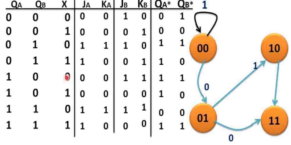
State Machines
In digital logic design, state machines are used to model systems with a finite number of states. They are often used in applications such as control systems, communication protocols, and digital circuits.
A state machine consists of a set of states, a set of inputs, a set of outputs, and a set of transitions between states. The transitions are triggered by the inputs and cause the machine to move from one state to another. The outputs are a function of the current state and the inputs.
State machines can be represented using state diagrams, which show the states and transitions between them. They can also be implemented using hardware or software.
State machines can be classified into two types: Mealy and Moore. In a Mealy machine, the output depends on both the current state and the inputs. In a Moore machine, the output depends only on the current state.
State machines can be designed using various methods, including truth tables, state diagrams, and state tables. The design process involves determining the states, inputs, and outputs, and then defining the transitions between the states.
State machines are useful for designing complex systems with a finite number of states. They provide a clear and concise way to model the behavior of a system, and can be implemented using hardware or software.
