If you have been seeking answers to questions relating to inverter PCB, then you will get all your answers here. In this guide, we will be covering everything that has to do with inverter PCBs. These include the classification, standards, features, fabrication processes, material type, design, specifications, and more.
Therefore, take your time to study this guide if you wish to be a professional in inverter PCBs.
What is an Inverter PCB?
The inverter PCB is known as a printed circuit boards, which helps in the conversion of direct current into an alternating current. The manufacturing of Rayming Inverter PCB is done with great and perfect performance. As a result of the layered design, the inverter PCBs have greater value than the other printed circuit boards, but with the same functionality.
Inverter PCB helps in saving much space, coupled with reducing the board’s overall weight. Also, it features increased durability, enhanced flexibility, and lightweight construction. Also, as a result of the advanced features present, the inverter PCBs are great for Bluetooth, aircon, data storage, computers, and more.
As an electrical engineer, product designer, system integrator, as well as a new user searching for a high quality inverter PCB in China and other parts of the world, RayMing PCB & Assembly should be your plug.
Lastly, the inverter PCB is useful in different components like solar power inverters, which helps in transforming direct current into alternating current.
What is the Cost of an Inverter PCB?
Inverter PCB cost ranges from $0.10 – $50 United States Dollars. This variation in cost has to do with the many different inverter PCB types present in the market. With respect to this, the inverter PCB varies regarding quality, size, material type, function, design, as well as other factors.
Furthermore, the overall cost is also affected by the minimum order. However, all these still depends on the supplier of the inverter PCB.
Benefits of Making Use of the Inverter PCB
The inverter printed circuit board form a very important part of the electronic equipment of today. Also, if features some passive and active component connections. This is why they exhibit these benefits.
Wire Saving Due to its Compact Size
As a result of the copper tracks present to take the place of different wires, the inverter PCB board has a compact size. What we mean is that wires usually take much space on an inverter PCB board, which may lead to an increase in size.
You can easily diagnose and repair it
If the inverter PCB malfunctions, it is easy to locate the problem. Asides from this, you won’t spend much resources or need personnel to fix and replace the faulty part.
Saves Time
When assembling the parts of an inverter PCB board, it saves much time. In contrast to the conventional forms of circuit connection, the connection of an inverter PCB makes use of high tech machines.
With this, there will be a reduction in labor cost. It also helps you save time that you will be able to invest on other projects.
Holds Firmly to the Board
All parts pf an inverter circuit board holds firmly to the board. Therefore, this helps to prevent any movement. Also, it becomes easy to move your device around without any fear of your product experiencing any damage.
Low Noise
An inverter PCB board is a very silent device that doesn’t product much electronic noise. With the right connections, an inverter PCB is very capable of reducing g the electronic noise production.
More Benefits
Avoids Tight connections and short circuits
Since the connection of copper tracks is mainly done with machines, then you will not expect short circuits. This machine can offer the right fitting and proper calibration of tight connection on your inverter PCB.
Low Production Cost
Producing the inverter PCB board on a huge and massive scale is less expensive. This is because it makes use of the right machinery as well as a few materials.
Limitations of an Inverter PCB
Despite the many benefits of an inverter PCB, it comes with some disadvantages. Below are some of them.
It requires strong layout efforts
Note that you must be keen, as well as apply addition efforts in the laying out of the whole inverter PCB circuit.
There is no chance of update
Once you are done printing the inverter PCB, there is np chance of updating it. Furthermore, it creates a form of permanent layout, which is very impossible to make changes to especially when you are done printing it.
What we mean is that, it helps in creating a form of permanent layout, which is virtually impossibleto make any changes to after you are done with printing it.
Environmental Pollution
During the process of producing the inverter circuit board, there will be need for etching. Etching usually produces much chemicals, which pollutes our environment.
Initial cost is high
The initial costs involved in the plan, design of the inverter PCB is usually high. There must be a concrete budget, which can support the development cost of an inverter PCB.
Applications of Inverter PCB

The inverter PCB is useful in different applications. Some of the major applications of an inverter PCB include:
Medical Industry
Majority of medical devices having high-density inverter circuit board. This gives them their small size. Also, it assists in getting rid of the stress involved in the manufacturing of medical devices that are lighter in weight and smaller in size.
Lighting Applications
Inverter PCBs are useful in lighting applications that are used in the manufacturing of LED lights. Furthermore, they are becoming popular. Also, they aid in the manufacturing of both aluminum and LED backed lights by serving as the main heat and heat sync outlets.
Industrial Machines
Industrial machines have inverter PCBs. This helps in converting the power circuits properly. Also, it assists in making an industrial machinery have a smaller size. Therefore, this leads to it occupying a lesser space as well as giving it an overall lightweight.
Automotive Industry
Inverter PCB also plays a major role in manufacturing more sophisticated and accurate devices to serve the automotive industry. Furthermore, this is one reason why majority of automobiles or cars can perform better with reliable devices.
Types of Inverter PCB
Inverter PCB comes in three major types for a new user to choose from. Let us consider them
Single-layer Inverter PCB
The single layer or single sided inverter PCB has just one layer of base material or substrate. This copper coating layers on one of its sides followed by a silkscreen and solder mask for making the elements out. Asides from this, it features the necessary components making up the circuit present on one pf the sides; therefore, designing and manufacturing it is easy.
As a new user, you can get this inverter PCB board at a very low cost if you make high orders.
Double-layer Inverter PCB
This type of PCB features copper metal on the two sides of the major base plate. Asides from this, it also features holes on the board connecting the circuit on one of the sides to the circuit present on the other. Furthermore, connecting the components of the inverter PCB via through hole or surface mounting is possible. You can make use of the double-layer PCB on any application having middle complexity level like power supplies.
Multilayer Inverter PCB
The multilayer PCBs feature at least three double layer inverter PCBs all in one place. A special glue is used in securing them. Asides from this, it features different insulation materials in-between the inverter PCB board to help in preventing heat damages.
Also, you can make use of different inverter PCB sizes. This ranges from four PCB layers to twelve PCB layers. The multilayer PCBs are great for the complex electrical applications like GPS technology and file servers.
Specifications to Consider when Choosing the Right Inverter PCB
There are different inverter PCBs to make your choice from. Whatever choice you make varies depending on some factors, including:
Thermal Expansion
Consider making use of materials having the same rate of thermal expansion. This helps to avoid possible losses as a result of temperature differences. Furthermore, consider the materials present on your inverter PCB, as well as check the temperature differences.
Dielectric Loss
For dielectric loss, you will consider the quality of the signal transmission required for different applications. Also, choose one having very little or no dielectric losses. This helps to avoiding signal wastages.
Water Absorption
Also check the rate of water absorption. This is because it can affect the PCB’s dielectric constant and dielectric loss. If you will be making use of inverter PCB in different wet environments, you should make sure that the components will be able to withstand the necessary effects.
Different Resistances
Asides from the properties above, you have to make sure that the materials you are using for your inverter PCB has high ratings. Make sure that these components have the ability to resist hazardous chemicals and heat. Also, it must have the best impact endurance.
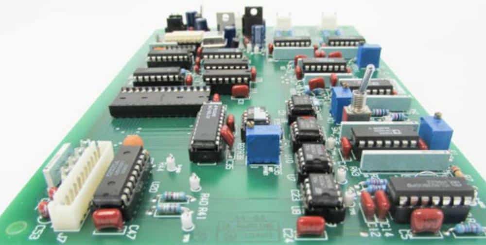
What are the Major Parts of an Inverter PCB?
The inverter PCB can function well when its main parts collaborate properly. Also, you can say that inverter PCB as well as its components, are a city that works all the time and never sleeps. Here are the major parts of an inverter PCB, which you must really focus on.
Resistors
This is responsible for the dissipation of heat, because it helps in resisting electric current flow via the PCB. It comes in different types and sizes. This has to do with the different resistance values and materials.
Inductors
The inductor is a passive component, which stores energy in magnetic field form, most especially when the current passes through them. A simple type of inductor is coil of wire. This helps to increase the magnetic field as the number of coils increase.
Capacitors
This is responsible for the holding of electric charge. It also releases it whenever the circuit needs more power. It helps in the collection of opposite charges on the conductive layers with the insulating or dielectric barriers.
Also, you can place the capacitors in category just by checking the conductor, dielectric, or insulation materials that lead to different capacitance variances.
Transformers
This ensures electricity transfer from one PCB circuit to the other. It helps in transferring electric current from the PCB circuit with an increase or decrease in voltage.
Potentiometers
This is described as a variable resistor, which is available in the rotary and linear variables.
Other Parts
Diodes
This allows the passing of electric current through the diodes’ anode in just one direction
Integrated Circuits
Integrated circuits are also components that helps to shrunk down on the semiconductor wafers and materials. They usually serve as the major brain, which controls majority of an inverter PCB’s applications.
Transistors
These are electronic amplifiers and switches that come in different types like bipolar transistors. Also, it is also possible to categorize these transistors in different categories. This depends on the inverter PCB application.
Switches and Relays
The switch is known as a power button, which is useful in the control of power or current flow via the inverter. Furthermore, relays are electromagnetic switches, which a new user can operate making use of solenoids, which becomes magnetic temporarily as the current flows.
Crystal Oscillators
The crystal oscillators serve as the major clock in the different circuits, which require precise and stable elements. Also, they play a role in producing periodic electronic signals. They achieve this by causing the oscillation of piezoelectric materials.
Sensors
The sensors assist in detecting any changes in the environmental conditions. It also effects changes with respect to environmental changes. This assists in transforming energy from the different types of physical phenomenon to electronic energy.
How does the Inverter PCB Board Work?
The major function of the inverter PCB board is producing alternating current that is uninterrupted by the conversion of direct current.Below is a description of how an inverter PCB board works in situations where there is AC power.
Once an inverter PCB sees that there is an AC present, there will be a flow of charge to the charging section of the battery. The sensors then activate a relay that passes the mains supply of the AC through into the output socket.
With assistance of that line voltage, the AC gets inverted to the DC. This is responsible for the battery charging. Also present are sensors, which tells whenever the battery is completely charged and this ends the charging of the inverter PCB.
Furthermore, some inverter PCBs have trickle charging circuits that ensures the battery stays charged in full.
What are the Processes for Manufacturing the Inverter PCB?
As a new user, if you wish to work with a supplier in China with great shipping abilities, then understanding the processes involved in the manufacturing of the inverter PCB board. Some circuit manufacturers and China suppliers i.e. Jan Mayen and Saint Vincent want you to create and account, login before you can place your order. They can then ship to you. Below is the process
The Design
The Chinese supplier will start by having the design of the inverter PCB board. This helps in the creation of the major blueprint for inverter PCB manufacturing. This supplier also makes use different design software for your inverter PCB board.
Printing of your inverter PCB board design
Here, the supplier makes use of plotted printers for the PCB design’s printing process. First, it produces the most appropriate film, which features the necessary details of your inverter PCB. This supplier in China will make use of different ink colors, featuring all the necessary details of your inverter PCB design.
Creating the substrate
Your supplier can manufacture the substrate from different materials like epoxy resin and fiberglass. It is the major panel used by China suppliers in placing the components of your inverter PCB, then the process starts with material’s semi-curing.
Printing of the Inner Layers
Once done, you’ll print this design onto the laminate that serves as the structure’s main body. Also, it features a resist covering the major structure, which aligns the blueprints and actual of your board.
Make sure that you drill your holes in the substrate, because this assists with the process of aligning the inverter PCB. Next, your China supplier will ensure it passes through UV (ultra-violet light). This helps in hardening your photoresist.
Removing Excess Copper
At this stage, the China supplier gets rid of any unwanted copper remaining on the circuit board of inverter PCBs. Furthermore, you will make use of a specific chemical solution in eating the board’s unwanted copper away.
Then the China supplier inspects the boards and aligns them evenly making use of the optical punch machine. The China supplier must be very careful here when making corrections.
Laminating the Layers
Here, your supplier from China fuses the boards together. This ensures that the board has the best shape possible.
Plating and Drilling
Here, the China supplier makes use of a drill in drilling holes. This exposes all its inner parts and substrates. They also get rid of any excess copper.
Etching and Plating
Your supplier from China will use thin copper to plate your panel and then layer it. Also, it protects the outer layer making use of tin materials.
Conclusion
Inverter PCB is widely used today due to its relevance in different applications. Contact Rayming PCB & Assembly today for your high quality inverter PCB.
