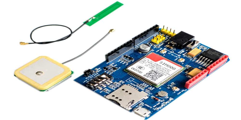
GPS technology has revolutionized the way we navigate and locate ourselves on the planet. However, the effectiveness of GPS signals depends on the design of the GPS antenna. A PCB (Printed Circuit Board) antenna is a popular choice for GPS antennas due to its compact size and ease of integration into electronic devices. PCB antennas are highly effective in receiving GPS signals and are widely used in various applications, including smartphones, wearables, and other portable devices.
The design of a PCB antenna for GPS requires careful consideration of several factors, including the size and shape of the antenna, the frequency of the GPS signal, and the impedance of the antenna. The antenna must be designed to resonate at the GPS frequency, which is around 1.575 GHz. The size of the antenna is also critical, as it should be small enough to fit into a device while still providing adequate signal strength. The shape of the antenna is also important, as it affects the radiation pattern and the efficiency of the antenna. In addition, the impedance of the antenna must match that of the GPS receiver to ensure maximum power transfer. Overall, the design of a PCB antenna for GPS requires a thorough understanding of antenna theory and practical experience in antenna design.
Design Considerations
When designing a GPS PCB antenna, there are several important considerations to keep in mind. These include the frequency range, polarization, and radiation pattern.
Frequency Range
GPS signals operate in the L1 and L2 frequency bands, which are centered around 1575.42 MHz and 1227.60 MHz, respectively. It is important to design the antenna to operate within these frequency ranges to ensure optimal performance.
Polarization
GPS signals are right-hand circularly polarized (RHCP). This means that the electric field vector rotates in a clockwise direction as the signal propagates. To receive these signals, the antenna must also be RHCP. It is important to ensure that the antenna is designed with the correct polarization to maximize signal strength.
Radiation Pattern
The radiation pattern of the antenna determines the directionality of the signal. In general, a GPS antenna should have a broad radiation pattern to ensure that it can receive signals from multiple satellites at once. However, it is also important to minimize any interference from nearby sources, such as other antennas or electronic devices.
To achieve the desired radiation pattern, the antenna can be designed with various features, such as a ground plane or a reflector. It is important to carefully consider the design of the antenna to ensure that it meets the desired radiation pattern and performance requirements.
In summary, when designing a GPS PCB antenna, it is important to consider the frequency range, polarization, and radiation pattern. By carefully considering these factors, it is possible to design an antenna that provides optimal performance and reliability.
Antenna Types

When it comes to GPS PCB antenna design, there are several types of antennas that can be used. Each type has its own unique advantages and disadvantages, and choosing the right one will depend on the specific requirements of your project.
Patch Antennas
Patch antennas are one of the most common types of antennas used in GPS PCB designs. They are relatively small and easy to integrate into a PCB layout, making them a popular choice for many applications. Patch antennas are typically made from a conductive material, such as copper, and are designed to resonate at the GPS frequency of 1575.42 MHz.
One of the main advantages of patch antennas is their directional nature, which allows for better signal reception in a specific direction. However, this also means that they are less effective at receiving signals from multiple directions simultaneously.
Helical Antennas
Helical antennas are another popular choice for GPS PCB designs. They are typically made from a coil of wire that is wound into a helix shape, with a small ground plane at the base. Helical antennas are known for their high gain and circular polarization, which makes them well-suited for applications where the antenna needs to be mounted at an angle or in a non-vertical orientation.
One of the main disadvantages of helical antennas is their larger size compared to patch antennas, which can make them more difficult to integrate into a PCB layout.
Dipole Antennas
Dipole antennas are a simple and relatively inexpensive type of antenna that can be used in GPS PCB designs. They consist of two conductive elements, such as wires or metal strips, that are placed parallel to each other. Dipole antennas are typically less directional than patch antennas, which can make them a good choice for applications where signals are coming from multiple directions.
However, dipole antennas are also less efficient than patch antennas, which means that they may not be the best choice for applications where signal strength is critical.
Overall, the choice of antenna type will depend on the specific requirements of your project. By understanding the advantages and disadvantages of each type, you can make an informed decision that will help ensure the success of your GPS PCB design.
PCB Layout
When designing a PCB antenna, the layout is a crucial element to get right. Here are some key considerations for the PCB layout:
Ground Plane
A solid ground plane is essential for the proper functioning of a GPS PCB antenna. The ground plane should be as large as possible and cover the entire PCB. It should also be placed on the opposite side of the PCB as the antenna trace. This ensures that the antenna trace is isolated and not affected by other signals on the PCB.
Trace Width and Spacing
The width and spacing of the antenna trace are critical to the performance of the GPS PCB antenna. The trace width should be kept as narrow as possible to reduce the impedance of the trace. However, it should also be wide enough to handle the required current. The spacing between the trace and the ground plane should be kept as small as possible to reduce the impedance of the antenna.
Via Placement
The placement of vias is also important when designing a PCB antenna. Vias should be placed as close to the antenna trace as possible to reduce the inductance of the trace. The vias should also be connected to the ground plane to ensure that the antenna is properly grounded.
In summary, when designing a PCB antenna, the layout is a crucial element to get right. A solid ground plane, proper trace width and spacing, and strategic via placement are all critical to the performance of the GPS PCB antenna.
Matching Circuit
Impedance Matching
Impedance matching is a crucial aspect of GPS PCB antenna design. The antenna and the receiver circuitry must have a proper impedance match to ensure maximum power transfer and minimize signal loss. The matching circuit can be designed using various techniques, including reactive matching, L-matching, and T-matching. The choice of the matching technique depends on the antenna’s input impedance and the receiver’s input impedance.
The reactive matching technique is the most commonly used technique for GPS PCB antenna design. It involves the use of capacitors and inductors to match the antenna’s impedance to the receiver’s impedance. The L-matching technique is another popular technique that involves the use of an inductor and a capacitor in a T-shaped configuration. The T-matching technique is similar to the L-matching technique but uses two inductors instead of one.
Balun Design
Baluns are used in GPS PCB antenna design to convert the single-ended signal from the antenna to a balanced signal that can be used by the receiver. The balanced signal has a lower noise level and better common-mode rejection than the single-ended signal. Baluns can be implemented using various techniques, including transformer-based baluns and microstrip baluns.
The transformer-based balun is the most commonly used technique for GPS PCB antenna design. It involves the use of a transformer to convert the single-ended signal to a balanced signal. The microstrip balun is another popular technique that involves the use of a microstrip line to convert the single-ended signal to a balanced signal.
In conclusion, the matching circuit is a critical component of GPS PCB antenna design. Impedance matching and balun design are two essential aspects of the matching circuit. The choice of the matching technique and the balun design technique depends on the antenna’s input impedance and the receiver’s input impedance.
Testing and Optimization

Once the GPS PCB antenna design is complete, it is crucial to test and optimize the performance of the antenna. This step is essential to ensure that the antenna meets the desired specifications and requirements.
To test the antenna, a GPS signal generator is used to simulate GPS signals. The signal generator is connected to the antenna, and the output is measured using a spectrum analyzer. The measured output is compared to the expected output to ensure that the antenna is working correctly.
During the testing phase, it is essential to optimize the antenna’s performance. This optimization can be achieved by adjusting the antenna’s dimensions and the ground plane’s shape and size. The optimization process is iterative, and several iterations may be required to achieve the desired performance.
To optimize the antenna, several parameters are considered, including return loss, gain, and radiation pattern. The return loss measures the amount of power reflected back to the source, while gain measures the amount of power radiated by the antenna. The radiation pattern is a graphical representation of the antenna’s directional properties.
In addition to adjusting the antenna’s dimensions and ground plane, other techniques can be used to optimize the antenna’s performance. For example, adding a matching network can improve the antenna’s impedance matching, while adding a balun can improve the antenna’s noise rejection.
Overall, testing and optimization are critical steps in the GPS PCB antenna design process. By carefully testing and optimizing the antenna, designers can ensure that the antenna meets the desired specifications and requirements, resulting in a high-performance and reliable GPS antenna.
Conclusion
In conclusion, designing a GPS PCB antenna requires careful consideration of various factors such as size, shape, and material. The antenna’s performance is highly dependent on the design, and it is essential to optimize it for maximum efficiency.
By following the guidelines outlined in this article, you can design a GPS PCB antenna that meets your requirements. It is important to note that the design process can be complex and time-consuming, but the results are worth the effort.
When designing a GPS PCB antenna, it is crucial to work with an experienced antenna designer who has a thorough understanding of the technology and can guide you through the design process. Additionally, it is essential to test the antenna thoroughly to ensure that it meets the desired specifications.
Overall, designing a GPS PCB antenna requires a combination of technical expertise and practical experience. By following the guidelines outlined in this article and working with an experienced antenna designer, you can design an antenna that meets your requirements and performs optimally.
