Printed Circuit Boards (PCBs) play a crucial role in modern electronics, providing essential infrastructure for devices across various industries. As electronic components shrink and performance demands increase, PCB technology has evolved to meet these challenges. One notable advancement is the adoption of High Density Interconnect (HDI) technology within PCB manufacturing, which has emerged as the ideal choice for a vast array of applications.
HDI technology increases interconnect density by incorporating smaller vias and thinner conductors, enabling more routes through a given area in a PCB. This not only allows for the accommodation of more components, but it also enhances signal integrity and reliability, meeting the growing performance requirements of today’s high-tech products. Additionally, HDI encourages design flexibility and can significantly reduce board size, resulting in cost savings and environmental benefits.
The decision to utilize HDI technology for PCB production should be carefully considered based on the specific needs and demands of an application. Ensuring compatibility with miniaturized components and heightened performance requirements, HDI proves to be an optimal choice for many manufacturers seeking the ideal PCB solution.
What Are PCBs
Printed Circuit Boards (PCBs) are the foundation of modern electronics, serving as the physical platform for electronic components and their connections. They’re typically made of fiberglass materials, with pathways etched or printed to allow electrical signals to flow between components.
Basic Components
PCBs consist of the following basic components:
- Substrate: The base material, usually fiberglass, which provides mechanical support for the components.
- Conductive Paths: Thin strips of conductive copper that form electrical connections between components.
- Components: Electronic parts such as resistors, capacitors, and integrated circuits (ICs) are mounted on the PCB.
Types of PCBs
There are several types of PCBs, each suited for different applications:
- Single-sided PCBs: These PCBs have components mounted on one side of the board, and copper pathways on only one side. They’re the simplest and most cost-effective option, but have limitations in signal complexity and density.
- Double-sided PCBs: Double-sided boards have copper pathways and components on both sides, connected by through-holes or vias. They offer more design flexibility and are suitable for moderately complex circuits.
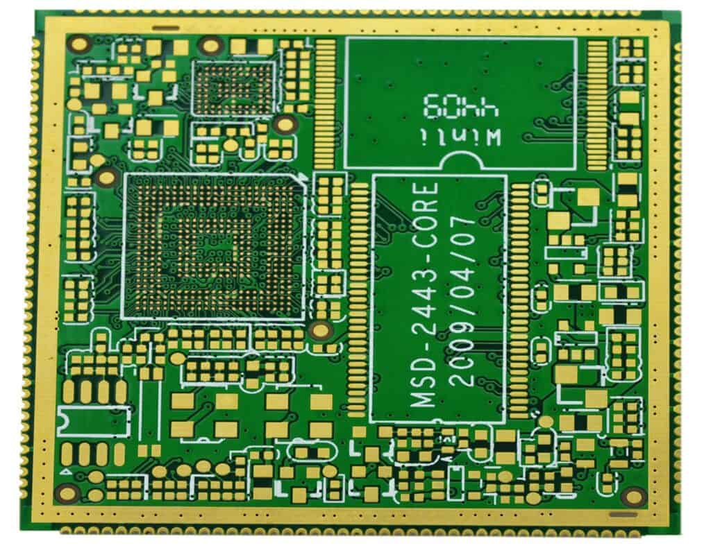
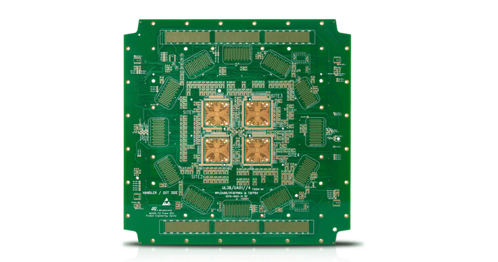
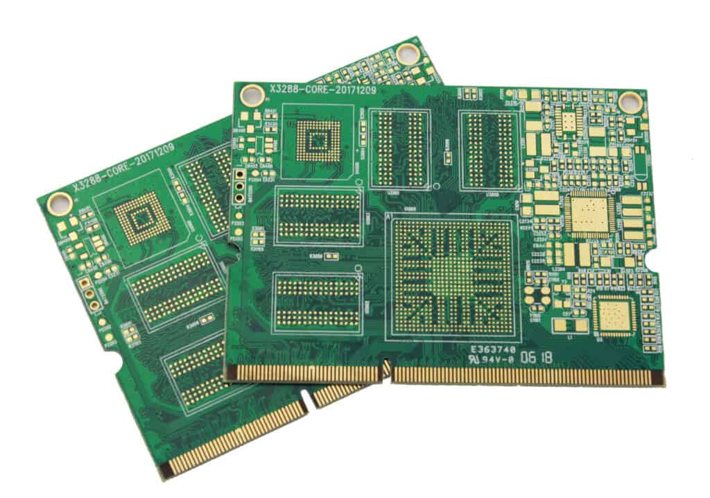
- Multi-layer PCBs: Comprising multiple layers of copper pathways, multi-layer PCBs enable complex signal routing and high density of components. They’re common in advanced electronics, such as computers and smartphones.
High-Density Interconnect (HDI) PCBs offer a promising solution for miniaturization, performance, and signal integrity demands in modern electronics. HDI boards feature thin dielectric material, fine copper lines, and smaller vias, enabling a higher density of components and connections, alongside improved signal performance. As a result, HDI PCBs are increasingly becoming the preferred choice for advanced electronic applications.
Understanding HDI Technology

High Density Interconnect (HDI) technology is an advanced method used in printed circuit board (PCB) design that addresses the increasing demand for smaller, lighter, and faster electronic devices. This sophisticated approach enables the manufacturing of ultra-small PCBs that have a higher circuitry density, improved performance, and reduced size.
Benefits of HDI
-
Smaller size: HDI technology allows for the miniaturization of PCBs. They require less space and are lighter, which makes them ideal for today’s compact and portable electronics.
-
Faster signals: HDI boards can accommodate shorter paths between components, resulting in reduced signal latency and faster performance.
-
Higher component density: With smaller vias, pad sizes, and traces, HDI enables a higher density of components to be placed on the board, allowing for more features to be integrated into the same area.
-
Improved reliability: The reduced size and increased density of components result in improved performance, reduced risk of signal noise, and increased overall reliability.
-
Cost-effective: HDI technology may help reduce overall production costs as it allows for more efficient use of materials, potentially requiring fewer PCB layers and a smaller overall board size.
Applications
HDI is used in a wide range of electronic devices, including:
-
Consumer electronics: HDI plays a crucial role in the development of compact gadgets such as smartphones, tablets, wearables, and gaming systems that require high-performance, lightweight, and compact components.
-
Automotive industry: Advanced safety systems, infotainment components, and electric vehicle control modules often use HDI technology to enhance performance.
-
Medical devices: Miniaturized medical equipment, implants, and diagnostic devices benefit from HDI’s improved performance and smaller size.
-
Aerospace and defense: HDI PCBs are used in various aerospace and defense applications, such as communication systems, guidance systems, and drones, where reliability and performance are critical.
-
Industrial automation: HDI technology helps meet the demands of industrial automation systems that require high-speed data transfer, smaller form factors, and reliable performance.
HDI technology has become increasingly popular as electronic devices continue to evolve. By offering an array of advantages, from increased component density to improved reliability, HDI plays a vital role in the ongoing development of advanced and miniaturized electronics.
Why HDI Will Be The Perfect Choice
Advanced Electronics Requirements
As technology advances, electronics require more complex and compact printed circuit boards (PCBs). High-density Interconnect (HDI) technology has emerged as a solution to meet these demands. HDI PCBs provide higher component density, allowing for more components to be placed within a smaller area. This leads to faster signal transmission and better overall performance when compared to traditional PCB designs.
Space and Weight Savings
Another advantage of HDI technology is the reduction in PCB size and weight. As electronic devices become smaller and more portable, reducing the size and weight of components is crucial. HDI PCBs allow for the use of smaller components and reduced layer counts, resulting in thinner boards. This not only saves space and weight within the device but also lowers manufacturing and shipping costs.
Improved Signal Integrity
Signal integrity is a major concern in electronic systems, and HDI technology can significantly improve it in various ways. Using HDI in PCBs reduces signal loss and interference, leading to enhanced signal performance. The shortened signal paths and reduced parasitic capacitance and inductance provided by HDI technology result in a lower noise environment and improved signal transmission quality. Furthermore, the optimized return paths offered by HDI PCBs contribute to better impedance management, which is essential for maintaining signal integrity in high-frequency applications.
In summary, HDI technology offers several benefits that make it an ideal choice for advanced electronics, including higher component density, space and weight savings, and improved signal integrity. By utilizing HDI in PCB design, manufacturers can create compact, high-performance electronic devices that meet the ever-increasing demands of the industry.
Limitations and Challenges of HDI
Manufacturing Complexities
HDI circuit boards have smaller features and higher density, making them more difficult to manufacture. In traditional PCBs, features like traces and vias are larger and easier to produce. As the board’s density increases with HDI, it becomes challenging to ensure consistency in manufacturing. Some complexities include the reduction of the allowable margins for errors and the requirement for advanced manufacturing equipment.
Higher Costs
The use of HDI technology usually results in a higher cost for the PCB. The increased manufacturing complexity and necessity for specialized tools and equipment contribute to the overall cost. Additionally, HDI boards may require more materials and a longer manufacturing time. Factors influencing the total cost of an HDI board:
- Advanced equipment demand
- Skilled personnel requirements
- Smaller tolerances
- More materials needed
While HDI technology offers several benefits, it comes with challenges. Manufacturers must balance the need for advanced technology with cost and manufacturing complexity considerations. Nonetheless, HDI continues to be a popular choice for various industries due to its advantages in performance and miniaturization.
Future of HDI and PCB Industry
The High-Density Interconnector (HDI) technology has made significant strides in recent years, playing a vital role in advancing the Printed Circuit Board (PCB) industry. As the demand for smaller, more efficient electronic devices continues to grow, HDI is becoming an essential tool in designing advanced PCBs.
One of the primary drivers behind the growth of HDI technology is the increasing need for miniaturization in electronics. As devices become smaller and more powerful, traditional PCB designs struggle to accommodate higher component densities. HDI PCBs, with their ability to support denser component layouts, help address this challenge by delivering more functionality in a smaller space.
The rise of the Internet of Things (IoT) is another factor fueling the growth of the HDI and PCB industry. IoT devices typically require compact designs and low power consumption, making HDI an ideal choice for these applications. As the IoT sector continues to expand, it’s expected that the demand for HDI PCBs will grow in parallel.
In terms of market trends, the following are some key aspects to consider:
-
Automotive sector: The automotive industry has been increasingly adopting advanced electronics for features such as autonomous driving, infotainment systems, and electric vehicle components. These applications require robust and reliable PCBs that can withstand harsh conditions, making HDI a popular choice for this sector.
-
Medical devices: Medical devices and equipment, including wearables and diagnostic tools, significantly benefit from HDI’s advantages in size reduction and performance enhancement. Smaller and lightweight devices are essential for improved patient experience and safety.
-
5G networks: The deployment of 5G networks worldwide necessitates the development of advanced communication equipment and infrastructure. HDI can provide the required high-frequency performance and reduced signal interference critical for 5G devices.
As the electronics industry evolves to push the boundaries of performance, size, and versatility, HDI technology will continue to advance and play an increasingly prominent role in the PCB industry. Manufacturers will need to adopt and adapt to these trends to maintain their competitive edge in the rapidly changing market landscape.
