Do you know that your electronics can operate at a higher speed, than they currently do? It will also interest you to know that the overall functionality of a consumer electronic device has a lot to do with the performance of the underlying foundation – the Printed Circuit Board (PCB).
In this article, we discuss the high speed board design, what it means and why it matters in the scheme of things.
The Definition of High Speed Board Design
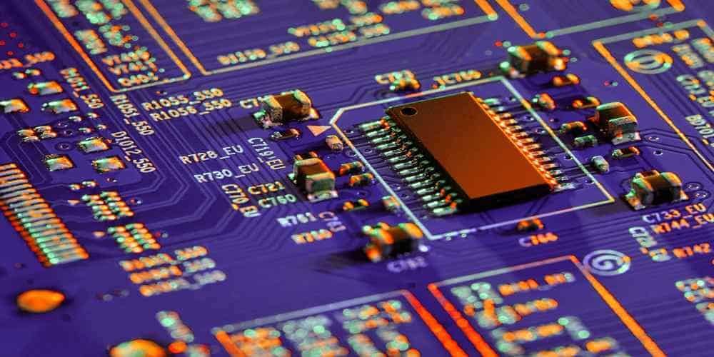
It means the type of Printed Circuit Board (PCB) that has been optimized to use the highest speed levels. The speed of the circuit is directly proportional to the pace at which the signals are transmitted through the board to the components.
The Need for Speed and Signal Integrity
Have you played the video game entitled, “Need for Speed?” You could see how the vehicles were equipped to accelerate at the highest levels. Likewise, something similar can be done to the consumer electronics, via the PCB.
The need for the high speed board design is because of many factors, but most especially, because of the need to facilitate the transmission of digital data between the circuit components.
Without this transmission, you can be sure that the components may not live up to expectations, as the required direction, in the form of data, has not be sent.
Another reason for using this circuit board design is to bolster the integrity of the signals. In this regard, there is a slight paradigm shift from the overt concentration on the routing and component placement options for the board. In this case, the focus is on the integrity of the signals, in the sense that it has to do with the following:
- Component Connection: the concentration here is on the types of components to be connected, taking into account the spacing.
- The proximity of the components to the signals is also considered. Ideally, these parts are not meant to be too close to the signals, both to avoid radiation emissions and signal disruption.
- The position of the traces on the circuit board is also considered.
How to Identify a High Speed Circuit Board Design
How do you know if the board has a higher speed than the conventional boards do? Here are some of the things to look for:
1. Check for the Applications
At a glance, you may be unable to find out if the board uses a high speed design process. However, a better way to figure it all out is by checking the target applications for the circuit.
The goal is to find out if the board is mainly dedicated for use with the devices that require a higher or advanced speeding process. It is only a PCB with a higher frequency that can match the use cases for the high-speed interfaces.
2. Check the Type of Interfaces Used
The type of interfaces on the board tells you whether it is optimized for more speed or not. For example, it is easy to tell a high-speed PCB if it uses the following interfaces:
- Thunderbolt
- HDMI
- Universal Serial Bus (USB)
- Ethernet
- PCI Express and;
- SATA
3. What Connects the Circuit?
Just like the PCB uses the wide range of high-speed interfaces, it is also possible to establish a connection between the PCB and the other sub-circuits using other high-speed interfaces. If that be the case, you should be able to find the following interfaces on the list:
- DDR3
- LVDS
- SDIO
- DSI and;
- CSI
4. The Signaling Frequency Leaves a Clue
Unsure if the PCB is made of a high-speed design? All you may need to do is to check the digital signal frequency.
Ideally, the high-speed circuit board uses at least the 50MHz digital signal frequency. It is also common for the signal rate to be above this figure.
Design Considerations & Rules for Making High-Speed PCBs

For the best possible results, you should stick to most of the industry rules and guidelines for the circuit board.
In case this is the first time you are hearing about these rules or you want to refresh your memory, here are some of the things to pay attention to:
1. Tuning the Trace Length
One major challenge to working on a high speed PCB is the noise that emanates from the board. Most times, the noise is because of avoidable factors, such as the close placement of the components and the inability to maintain the right trace length.
For this reason, it is imperative to tune, reduce or keep the length of the trace at the barest minimum. Doing this helps to reduce the chances of causing noise problem in the transmission lines.
The following recommendations are helpful in this regard:
- Maintaining a trace length of under 4.5 cm or less than 65 ohms, which helps to maintain the delay within 940 ps. This is peculiar to the SDRAMC-related signals, most especially for the 3.0-volt memory bus.
- A trace length of less than 55 ohms (under 4 cm), can also be maintained for the SDRAMC-related signals for the 1.8-volt memory bus. This also helps in maintaining the delay within 800 ps.
2. Ground Bounce Reduction
Although the primary function of the high speed PCB is to bolster the speed at which signals and data are being transmitted. Yet, this could come at some expense, especially for the decrease of the output switching times.
In that case, the devices would now be working with the faster switching times, which are now in place to match up with the fastness of the devices.
The outcome is usually a higher transient current in the outputs, especially as they discharge the load capacitances. It is when these happen that the PCB can be said to be susceptible to a phenomenon called “Ground Bounce.”
The goal is to reduce the ground bounce using a wide range of techniques. The reduction processes include but are not limited to:
- Making an individual connection of either the via or ground pin to the ground plane.
- The ground bounce can also be reduced via the use of wide and shortened traces, which must be between the capacitor pads and via. Rather than using only the traces, you may opt to position the via adjacent to the capacitor pad.
- Another efficient method of reducing ground bounce on the board is to maintain a wide, yet short length for the traces that stretch from the power pins to the power plane. The idea is to reduce the series inductance – a model that also aids in the reduction of the transient voltage drops from the power plane to the power pin.
3. The Prevention of Crosstalk
Crosstalk is one of the aftermaths of on-board noise. As a source of noise on the PCB, it is imperative to nip it in the bud to avoid interfering with the board’s performance.
Before talking about how to reduce the impact, let us first understand what it means.
Crosstalk is a type of on-board noise source that emanates due to the unwanted coupling or combination of signals between the parallel traces.
The following processes, when put in place, can help reduce crosstalk in the high speed circuit boards:
- Perpendicular Trace Routing: this is the basic process of reducing crosstalk. It has to do with the reduction of the distance between the adjacent plane and the signal layer. It also has to do with the increase in the distance between the two signal layers. However, note that this process works best for the dual-stripline layouts.
- Conductor-to-Ground-Plane Proximity: you may also consider designing the transmission line in a way that its conductor is positioned close to the ground plane. This is one process that helps couple the transmission line tightly to the ground plane, while aiding the decoupling from the adjacent signals.
- Single-Ended Signal Routing: it is also possible to route or connect the single-ended signals. Follow this process if there is a significant coupling of the signals. The routing process involves connecting the single-ended signals on the different layers, and making the layering process “orthogonal” to each other.
- Signal Lines’ Spacing: try to widen or space out the signal lines. This should be done as much as the routing restrictions would allow. The rule of thumb is to maintain a spacing of “3 times the dielectric height.”
4. Where to Place the Components
Although components are mapped via the schematics, it is important to ensure they are not interfering with the circuit board’s workings.
Where you place, mount or position the components is very important. With the schematics, you can do the following to ensure an accurate placement of the components:
- Component Placement at the Center: it is better to place the high-speed interfacing components at the board’s center. The reason is that the centered positioning helps to distance these parts from the board’s edge. Otherwise, having these types of parts closer to the PCB’s edge tends to negatively influence the signal transmission.
- Spacing Considerations: just as we spaced or distanced the high-speed components from the edge, we should also consider the length of the traces. Due to the shortened length of the traces, enough space should be left behind to enable the accuracy of the length tuning process.
- Analog Component Separation: the analog components should be separated from the traces and the digital components. Doing that helps to reduce the chances of Electromagnetic Interference (EMI). Also, if there are any analog components on the board, they should be designated to a separate Ground (GND) polygon.
5. Consider the Termination Schemes
These have to do with the signal reflection or the tendency of the signals to “bounce back” on the board. Usually, the termination or the constant back and forth reflection of the signals along the transmission lines is commonly caused by the mismatching of the impedance.
There are different signal termination schemes, including:
- Series Termination: this has to do with the matching of the resistor to the impedance at the “signal source” instead of at the “load.” Although the downside to this is the increased RC time constant degrades the rise time, it does have a benefit – the consumption of little power.
- Active Parallel Termination: this has to do with the selection of the voltage for the output drivers to draw the current from the high and low-signal levels. It would require a separate voltage source to match the output transfer rates via the sinking and sourcing of currents.
- Series-RC Parallel Termination: it uses the capacitor and resistor network to act as the “terminating impedance.” The major consideration is the size of the capacitor. As much as the capacitor is expected to be large enough to filter the DC’s flow, it also needs to have an ideal sizing that doesn’t prevent the signals from going beyond the threshold.
- Simple Parellel Termination: as the name suggests, it is one of the simplest termination schemes for the high speed PCB. It has to do with the equality between the line impedance and the Terminating Resistor (RT). It is also possible to position the “terminator resistor” close to the load.
- Thevenin Parallel Termination: the structure involves the tying of the resistors between the Ground (GND) and the VCC. This leads to the addition of the current drawn from the power supply. By using the “Thevenin Voltage Divider,” it is possible to split the terminator resistor between the R1 and R2. The significant upside to this termination scheme is the reduction of the current gotten from the source device.
Do You Need a High-Speed PCB?
The point is that using a high speed board design doesn’t have to a consideration if there is no need for it. Due to the design of most circuit boards, however, it has become necessary to use this model.
Here is why you may consider integrating high-speed designs into your circuit board projects:
1. The Type of PCB Substrate
What type of material do you use for the PCB? The point is that the substrate materials tend to contribute to the signal integrity issues on the board. It has a lot to do with the relative dielectric constant value of the material.
2. Signal Integrity Issues
The major consideration is the generation of signal integrity problems, as accentuated by the distortions encountered along the way.
Ordinarily, the signals don’t follow the ideal process of moving from the source (Tx) to the load (Rx) without interferences. The interferences or distortions along the way are chiefly caused by factors like:
- Electromagnetic Interference (EMI)
- Switching issues
- Mismatched impedance
- Attenuation
- Signal “bouncing back” (reflection) and;
- Crosstalk
With these factors, tips & tricks and excellent technology at our disposal, we help you manufacture high speed boards that are free of the common challenges in today’s PCBs. Contact us today.
