In today’s world, smaller devices are very common. Most industries use smaller hardware products due to their benefits. Smaller is better when it comes to modern hardware products. A mini circuit board is the core of smaller electronic devices. This board is very vital for wearable technology.
Mini PCB are commonly used in devices like mobile phones and wearables. By nature, these devices are compact and small. Therefore, there is a need for a mini PCB. These boards have made the production of smaller devices easier. This article provides vital and well-detailed information about mini PCBs.
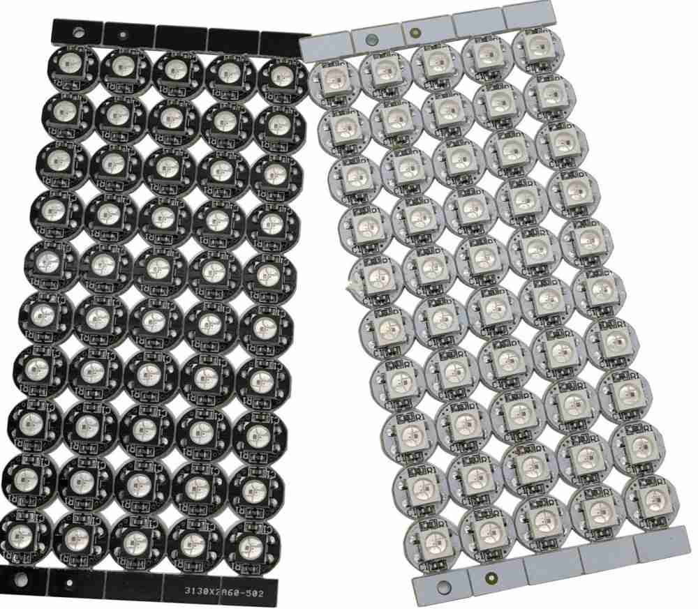
What is a Mini LED PCB?
A mini LED PCB features a grain size of almost 100 microns. The mini LED falls between the Micro LED and traditional LED. It is a better version based on the typical LED backlight. The Mini LED is also called a sub-millimeter LED.
The yield rate of the mini LED is much higher than that of the micro LED. Mini LED features unique-shaped cutting characteristics. This LED can get a high-curved backlight with a flexible substrate. The mini LED incorporates a dimming design and features better color rendering. This feature can bring LCD panels. The mini LED also features more refined HDR partitions which can save a large percentage of power.
So, this LED is ideal for backlight applications like HDR and special-shaped displays. The mini LED is also ideal for some consumer electronics.
Theoretically, mini LED requires a less technical process. It is easier to accomplish mass production. This LED can help to create a large number of LCD backlight markets. For an LCD TV panel featuring a Mini LED backlight design, the price is almost 80% of an OLED TV panel. However, the picture quality and brightness are similar to OLED’s.
For example, a 55-inch Mini LED backlight LCD panel features LEDs of 40,000. This will help LED manufacturers to minimize their production capacity.
In terms of picture quality, micro LEDs have better qualitative improvements. This LED is the next set of revolutionary display technology. However, the present technology is immature. Mini LED is an enhanced version of LED backlight. This LED is expected to be the market’s mainstream.
Mini Circuit Boards Used for Small Applications

Your PCB design determines a whole lot about your PCB. One of such is the size of your board. A computer-aided design program can help to create the PCB layout. This will help you reduce the board’s size. In most cases, the spaces between two conducting paths are 0.006 inches or below.
The circuitry and the enclosures housing the PCB will determine the PCB dimensions. These factors will also determine the fixed components of the PCB. Effective software can help you reduce the size of the PCB easily.
The size of your PCB depends on the space of the enclosure. You will need a mini circuit board if you are designing a tiny device. Most mini devices feature mini circuit boards. However, creating a mini circuit board design requires having small components. This means the components will be soldered with a fine tip soldering iron. Also, the manufacturer will need microscope glasses.
Applications of mini circuit boards
Mini PCBs are widely used in several applications. Most times, these circuit boards are available in mini devices. Mini circuit boards are ideal for use in the applications below:
- Semiconductor
- LED
- Instrumentation
- Industrial
- Contract manufacturing
- Power electronics
Tips to Create a Mini PCB
Designers need to consider certain factors when designing a PCB. These factors include:
- Minimum silkscreen width
- SMT minimum solder mask width
- Minimum trace width
- Minimum vias space
- Drilling and finishing hole
- Minimum solder mask clearance
The minimum size of the PCB will depend on these factors.
You should determine the buried and blind vias carefully. These vias can have a significant effect on your design. They can also determine how small your PCB would be.
Vias help to connect traces between PCB layers. Also, traditional options help to minimize the routing space available in any PCB. Avoid using a bigger board size to maximize routing space. It is advisable you check for other alternatives.
Blind vias help to connect internal and external layers with less spacing. Buried vias can help to connect several internal layers. However, they don’t extend to an external layer. This reduces the space requirement and provides a more stable PCB.
Manufacturers need to consider the issue of cost when it comes to buried and blind vias. It is more complex to fabricate buried and blind vias. Therefore, this increases the cost of the circuit board. The cost will reduce to a certain level if there is high volume production.
Also, you need to take the spacing between the components into consideration. When components are too close, this might hinder trace routing. Components with more pins will require more spacing. Appropriate spacing will make component soldering on the PCB easier.
Furthermore, the designer should ensure components adhere to a standard pin numbering design. This will make everything equally organized. Also, this will reduce the probability of errors during soldering. Doing this will help you to reduce any manufacturing concerns.
Advantages of Mini PCB
Nowadays, electronic products are constantly miniaturized. As technologies improve, more companies produce smaller and more compact devices. Unarguably, one of the reasons for producing smaller electronics is to save space. The miniaturization of electronic devices offers a wide range of benefits. Mini PCBs are useful in the production of smaller devices. Below are some advantages of mini PCBs:
Space saving
Mini PCBs are ideal for smaller devices like mobile phones. In smaller devices, the manufacturer will fit the circuit board and other components. For instance, a mobile phone comprises other parts like a camera, battery, and more. So, mini circuit boards can save up some space on a device.
Reduced cost
Miniaturization helps to reduce the materials needed for producing a device. Making use of fewer materials has some cost-saving benefits. One of these benefits is the lower cost of transportation. You can transport smaller products for a reduced price. Also, Mini circuit boards require less cost to produce. Therefore, using mini PCBs can minimize the cost of electronic production.
Environmentally friendly
The production of mini circuit boards requires fewer materials. Therefore, this is beneficial to the environment. The use of fewer materials will result in less waste.
Efficiency
Mini PCBs are very efficient. These boards offer great dissipation benefits. This is one of the major reasons they are commonly used in consumer electronics. These boards also feature great electrical and thermal properties.
Creating a Mini PCB Board Size: How to Reduce the Size of Your PCB
Technology continues to get smaller, and for sure we have to get prepared that this continues to be the case into the future. Layout engineers and designers are under pressure constantly to reduce the size of the board. Therefore, we will be taking you through five methods that will help in shrinking your printed circuit boards.
Removal of Testing Tools
The early board drafts usually include headers, extraneous pads, and components that make testing and debugging easier. Immediately you are set to scale down the board to the least possible size, these should go first.
Now, there’s no need to add a whole header to off-board debuggers before checking with your oscilloscope. Although, you may require some pads that are exposed if you will be subjecting your product to the bed-of-nails verification type.
Making Use of Multilayer circuit boards
So many prototypes are achieved as one or two layer boards. With this, you will get surface access to the traces and components. This enables circuit testing, rework, and repairs. Once you’re satisfied with your mini PCB board design and set to shrink or reduce, moving the components altogether can do so much. This is because you will still require room to route.
Transferring to a board of four layers is not as difficult as you think. It gives much room to run your traces ensuring that less space is taken on the outermost layers.
Bluetooth Wi-Fi Combo Module
Many benefits and pitfalls follow the use of modules compared to discrete solutions for anything regarding your board, either wireless connectivity or power conversion. Usually, this decision comes early during the process of design. Although, there are times you will discover that this discrete cost effective solution is so expensive and you decide to make your switch.
What this means is combining Bluetooth and Wi-Fi into one module using an integrated antenna.
Circuit Boards Having Heavy Copper
Allocating a large amount of area of your printed circuit board to traces of high current or thermal management, means that you can use heavier copper to shrink your board. Most people usually consider the minimum width of the trace. However, more focus should be on the total area of the trace.
A PCB’s copper layer is usually 1oz. Therefore, doubling this thickness to make 2oz allows you to run traces that are half as wide having similar current capacity. Majority of board houses can easily handle the common upgrade 2oz; however, there is thicker copper present.
The industry usually considers any heavy copper that falls between 4oz – 10oz. However, boards can be composed of copper of about 200 oz.
Customize the Size of your circuit board: Length and Width
At times, the board’s height has a much tighter restriction compared to the length or width. However, this could become a problem if your design utilizes tall components such as headers or electrolytic capacitors. When the headroom is limited, headers accepting wires at ninety degrees could be a great solution.
If your style is being crampled by a huge capacitor, It is possible that you can split the capacitance across much smaller components that are placed close together. Using this tactic doesn’t mean that cost will be reduced. However, this could give you the needed clearance in a small and tight space.
Making use of a smaller size for your capacitor and resistor
Since the initial versions of circuits are typically populated by hand, it is advisable to use 0805 capacitors and resistors having lots of clearance. This is because handling it is easier. Also, they provide more space to ensure that their designator is marked on the silkscreen.
Immediately the design is set for compression, you can go ahead to reduce the component’s package size. Though there are tiny components such as the Panasonic’s line composed of 01005 resistors, as well as you pulling ridiculous stunts such as putting resistors on its narrow side instead of being made to lie on the board flat, it is very rare to go below 0402.
Pick and place machines of standard features have a great success rate having 0402 packages. However, as regards smaller components, they may struggle and decrease your product’s overall yield. The component’s power rating also seems to decrease with respect to size. Usually, your design may not accept this.
Shrinking the Circuit Footprints
Immediately you have successfully shrunk the board’s components as far as you can, it may be possible for you to make things tighter if you change your footprints. Footprints do not really define tolerances, as they serve mechanical drawings, and could err on the generosity side.
Common footprint defaults such as 0805 have to cover many variations possible. Therefore, they could be bigger than what you need for the design. Check each specific component’s datasheets to see the amount of room to be left for each of the pads and then modify the design accordingly.
Conclusion
Without any doubt, mini circuit boards offer a lot of benefits. These boards have proved to be useful in the production of smaller devices. Mini PCBs play a significant role in today’s electronic industry. Buried and blind vias help to reduce the size of a circuit board. These vias allow mini boards to be packed tighter.
Although mini circuit boards are small in size, they can be complex to fabricate. Therefore, manufacturers need to pay attention during their fabrication process.
