There are different types of PCBs. The double sided PCB is one of them. Since PCB is the foundational material of most electronic devices, it is important to understand their types. Double sided circuit boards play significant roles in several electronic applications. They are featured by both intermediate and complex circuitry. These PCBs are also ideal for use in several applications. We will discuss essential facts about this PCB type in this article.
What is a Double Sided PCB?
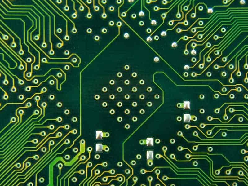
A double sided PCB is a type of circuit that features two sided paths or traces. This board has a bottom layer and a top layer. It is a circuit board featuring copper layers on both sides. Manufacturers use holes to connect circuits on one side to the other side of the board. A double sided board is also known as a 2 layer PCB or a dual layer PCB.
Electronic components on a double sided circuit can be connected using two types of technologies. These technologies are Surface Mount Technology (SMT) and Through Hole Technology (THT). THT passes the small wire via the holes to join several components. SMT doesn’t use wires to connect components.
In a 2 layer PCB, conductive copper and electronic components can be mounted on both sides of the board. This will help the traces to be across each other. A 2 layer bare PCB helps manufacturers to design more complex boards. The two sides of this board are clad with conductive material.
Manufacturers apply a solder mask on the two sides of the circuit. Since two conductive layers make up the circuit, it is known as a two layer PCB. The base of this PCB is made of an insulating material. A double sided PCB can feature traces on both sides while components are mounted on one side. It has an increased level of reliable connections.
Dual Layer PCB Manufacturing
The manufacturing process of the double sided PCB is a very complex task. However, this process can be simple and straightforward if manufacturers abide by certain rules. The substrates used in a 2 layer PCB varies. This depends on the application requirements. Manufacturers apply solder mask to the two sides of the layer. This will serve as a shield to the copper foil.
After the solder mask has been applied, manufacturers place a silkscreen on both sides of the circuit. The silkscreen serves as a reference indicator for mounting electronic components on a board. It includes important information of the board. The silkscreen is used for adding characters and symbols on the board. The copper layers used for a dual layer board cab vary in thickness.
Therefore, the construction of a dual layer PCB includes;
- Copper layer
- Adhesive layer
- Dielectric layer
- Adhesive layer
- Copper layer
Steps in Manufacturing Dual Layer PCB
The steps will guide you in manufacturing a functional dual layer PCB below;
- Use a PCB designing tool to create the top and bottom layout of the circuit board.
- Print out the layouts on a quality glossy paper.
- Cut the copper plated fiberglass PCB substrate to the specified dimension or size
- Iron the top layout print on the top side of the PCB using a cloth iron.
- Use a scrubber to remove the laser ink from the circuit board Tracks
- Drill the component holes
- Clean out unwanted substances on the other side of the board
- Print the bottom layout of the circuit board. Ensure you align the layouts of the board properly.
- Put the board in a chemical solution to etch out the copper. The chemical solution used for this purpose is copper chloride.
- Use conductive ink to create the plate through hole.
- Apply solder maskon the two sides of the circuit board.
- Solder the electronic components
What is a Double Sided PCB Board?
The double sided PCB board is the blank board used for the double sided PCB. This board has no electronic components mounted on it. It is a core material for the production of the double sided circuit board. This bare board is used to mount electronic components. It provides electrical and mechanical support for a circuit.
A double sided circuit board features all electronic components. This circuit board is used in the manufacturing of several electronic devices. The double sided PCB board is a laminate sheet that features no electronic components.
Most people confuse the double sided PCB board with the circuit board itself. It is important you know the difference between these two materials. This board is regarded as the foundation of a dual layer PCB. The double sided PCB board provides electrical connection and mechanical support to electronic components using signal traces and conductive pathways.
The Benefits of a 2 Layer PCB
In recent technology, there has been more demand for a 2 layer PCB. This is because of the benefits it offers. This type of PCB is one of the most popular PCBs in the electronics industry.
A 2 layer PCB provides heat dissipation. The extra layer of copper on this PCB enhances heat dissipation. During the engraving procedure, enough copper is eliminated to make the tracks. Therefore, the extra copper remains in the circuit. Manufacturers prefer this board since it makes it easy to create various conductive paths on a circuit.
A 2 layer PCB features two conductive sides that enable the assembly of large components. This circuit board also enables maximum use of available space. There is space for electronic components on the two sides of the circuit. Double sided boards help to duplicate power tracks.
The Use of Ground Planes in a Two Layer PCB
Manufacturers need to understand the use of ground planes in a two layer PCB. Placing a ground plane in a 2 layer PCB design helps to achieve functionality. Most PCB designers have difficulties in implementing a ground plane on their 2 layer circuit.
Adding a ground plane to your two layer PCB is the best way to achieve signal integrity. To protect your circuit from EMI, you can separate a ground plane from the signal layer. One way to reduce EMI vulnerability is to route a return trace to a signal trace in an adjacent way. Including a ground plane on the bottom layer of a 2 layer circuit reduces loop inductance.
Typically, manufacturers should position signal traces very close to the ground plane. This will help to reduce crosstalk between traces. A good technique to use for a 2 layer PCB is gridding. This is better than placing a continuous ground plane across the bottom layer. Gridding involves routing the ground and power traces in a differential way. Here, the manufacturer imitates a pair of power lines.
Gridding provides a good level of noise reduction for your double sided PCB. Another solution is incorporating two perpendicular grid patterns on the two layers. The manufacturer use vias to connect the grids at points where they cross. This helps to ensure all the grid sections have the same potential.
Some 2 layer PCB ground plane designs are more likely to use analog and digital signaling on the same board. You can separate the ground plane into an analog section and a digital section.
Design Guidelines for a Two Layer PCB
These design guidelines will help to minimize the risk of crosstalk or switching noise.
Route ground return on layer 1 and electronic components, power and signal paths on layer 2
The goal here is to make use of continuous return path under the signal path. You can achieve this by using a ground plane on the board’s bottom layer. The top layer will then feature all the components. This makes it quite easy to trace the signal routes. You will be able to identify which traces are power and the ones that are signals through their line width.
Make your cross-under short when routing on the bottom layer. If you can’t shorten it, put a return strap over it.
It is important to make the impedance path low for every signal line in a 2 layer PCB design. This will result in having a low mutual inductance between signal-return paths. Ensure there is an isolation gap around the ground plane when routing a signal line. The signal traces you routed beyond this gap will detect a gap in the return path. This will help to provide crosstalk to signals crossing the gap. Make the gaps short to reduce this problem.
Use 13 mil drilled diameter, 6 mil wide signal trace, and 20 mil wide power traces
You will achieve the best 2 layer PCB design if you adhere to this guideline. PCB designers always want to achieve highest routing density at a low cost. A 6 mil wide trace might seem narrow for a signal line. But, this wide trace is capable of carrying 1 A of DC current without an increase in discernable temperature. A 20 mil wide trace can carry 3 A of DC current without noticeable rise in temperature.
Route signal traces very far apart
Ensure you route signals far apart to minimize cross talk. Signal traces feature high characteristics impedance. There can be some cross talk between traces since they are not close to the return plane. The cross talk is more if the space between adjacent signals is closer. The farther the signal traces, the less the cross talk.
Assign one return path for every digital signal on all connectors
When several signals share the same return pin, this contributes to switching noise. Multiple signals may share only one or two return pins in many connectors. This will definitely cause switching noise or ground bounce.
Avoid using copper fill
Using copper fill won’t solve any problem. Copper fill are most likely to create more issues. A 2 layer PCB designer should rather route power as traces. You will be able to check the power paths to ensure connectivity. Utilize the bottom layer as ground if you are using a ground fill. You can’t minimize cross talk by including copper fill.
Double Sided PCB Manufacturer
A double sided PCB manufacturer is charged with the responsibility of creating a good circuit. This manufacturer uses special programs to design and manufacture a two layer board. It is important the manufacturer complies with existing rules of 2 layer PCB manufacturing. The PCB manufacturer creates a dual layer circuit using the additive and subtractive methods.
In the additive method, the manufacturer applies the foil pattern on the circuit chemically. The subtractive method uses a layer of foil to cover the surface. After this, the manufacturer removes unnecessary places from it. Another role a PCB manufacturer plays is performing an electric test. This test is an important step in the production process. Other roles the manufacturer performs include;
- Installing all electronic components
- Checking the functionality of the components
- Cross-checking the location and pattern of holes
- Inspecting the application of solder paste
- Arranging elements on the circuit board properly
- Soldering quality control
Frequently Asked Questions
What is the maximum distance between the components on a 2 layer PCB?
There is no maximum distance between the electronic components on a dual layer PCB. The distance between these components is determined by the application requirement.
Does a double sided circuit board have limitations?
Yes, a double sided circuit board has its setbacks. This board isn’t suitable for applications that conduct heavy current. Also, this board has a high risk of overheating when it is being soldered. A double sided board can also be very difficult to fabricate.
Conclusion
Double sided PCBs are commonly used in the production of some electronic devices. Not only do they offer high signal transmission, they also help to design the most compact device. The manufacturing of these boards is cost-effective; hence, it is a great choice. The dual layer PCB provides more possibilities for complex devices. This article has provided well-detailed information as regards a dual layer PCB.
