A Printed Circuit Board (PCB) is said to be operating at a higher voltage when it goes above the recommended rating for traditional circuit boards.
If you have been wondering about the rating at which the board operates, some of the reasons for preferring it and design considerations, this article will answer all of your questions.
Let’s Understand the Concept
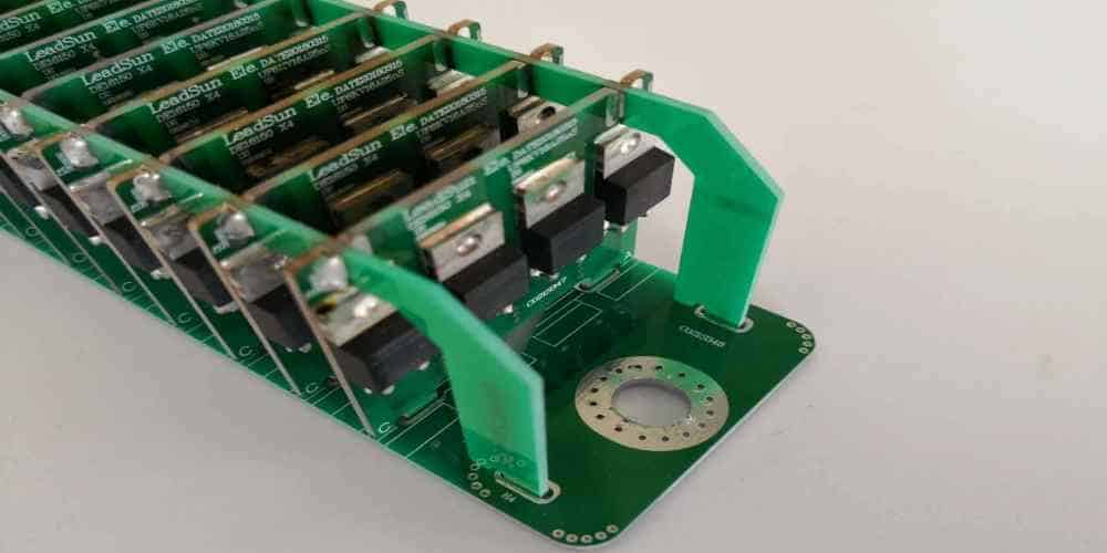
By the name, you can tell that it is a dedicated PCB that operates at a higher voltage. Another point is that the increase in voltage is proportional to the workings of the target devices. This is why this PCB is commonly used to build the foundation for Electric Vehicle (EV) charges, power supplies and inverters. These applications use up more power and therefore, needs a circuit that boosts the performance.
What is the Rating for High Voltage PCBs?
This is where there is a bit of confusion. Some people are not sure of the actual rating or voltage capacity of the circuit board.
The point is that there is yet-to-be an official value or rating for the high voltage PCB design. That notwithstanding, designers often work with the above 100-volts benchmark. Thus, any circuit that operates higher than 100 volts can best be described as a high voltage PCB.
Balancing the Power Rating with the Design
Naturally, since the board performances at a higher pace, you can expect it not to toe the line of the traditional PCBs that operate at a lower voltage.
This lends credence to the need to have the design optimized accordingly. These points boost the reason why the design optimization is important:
- There is the need to modify the PCB to work in line with the higher application requirements.
- A high voltage circuit consumes more power. Working with the minimal design capacities for the regular boards would only expose it to falling apart or crumbling, due to the heavy loads it now carries.
Best Practices for Making High Voltage PCBs
You don’t just dabble into designing these boards. Following some of the industry-related steps is recommended – for the best results.
Here are some of the best practices you want to follow:
Internal Layering
The possibility is there to integrate a multilayered structure into the PCB’s layers. This can be achieved via the use of medium voltage on all the layers.
Here are some of the things to have in mind when doing this:
- Material Selection: the standard prepreg Flame Retardant 4 (FR-4) multilayered PCB material must be avoided for this design. It is not perfect for the medium-to-high voltage PCB design due to the homogenous internal structure and the fragility.
- Spacing Options: there should be at least 0.005-inch of thickness between the separated layers. This enables the proper filing of the spaces between the layers.
Routing Capabilities
The traces must be properly routed or connected to help achieve the desired results. The following tips should help you make the most out of it:
- High-voltage traces should not be routed or connected through the board’s internal layers.
- There should be a need to integrate “clearance” between the traces, especially if these traces have a higher voltage difference between them.
- Sharp edges and turns should be avoided in the high voltage PCB design. The avoidance is to help reduce the chances of their acting as the “areas of concentrated electric field.”
Take Note of the Disruptions
Printed Circuit Boards (PCBs) are often susceptible to disruptions, in the form of Electromagnetic Interferences (EMIs). The emission of distortions over a wide spectrum is a huge challenge to the high-voltage circuit’s performance.
The EMI considerations go both ways – they can be internal or external. For the internal, we are looking at the likes of component placement and routing. For the external, we are considering the devices and environments that can potentially disrupt the circuit’s signals.
A good way to start is by having a firm control over the internal disruptors. The following should be done:
- Pot the high-voltage components and shield them with a metallic sheet.
- Make an extensive via stitching to the ground plane and;
- Have a small loop area on the board.
Polygon Plane Clearance
This has to do with the extension of the polygon plane clearance, up to board’s sections. It is also important to ensure the non-implementation of small spacing or high-voltage, between the internal planes on a multilayered PCB.
Top Considerations for the High Voltage PCB Design

There is a difference between the design concepts/best practices and the considerations. While the former acts as a guide to help you get the best results, the latter helps you to make informed decisions.
With that being said, here are some of the things you wish to have in mind when designing a high-voltage circuit board:
1. Reduce Arcing through Isolation
You must note that the components on the board vary by the voltages they use. If you are using the ones with a higher voltage, it makes sense to keep them safer from influencing the other components’ performances, negatively.
The best way to go about this is by isolating the high-voltage areas. These points will help you make the best partitioning:
- Circuitry Grouping: start by placing the high-voltage circuits into a group. Doing this helps to keep the same voltages in one box and therefore, minimize the likely negative impacts they would have had if they were allowed to interface with the other PCB components.
- Insertion-Making: the best way to physically isolate the “high-voltage areas” is by adding an insert to demarcate these areas from the rest of the board. The slot to be routed out should also be placed close to the insert.
2. Noise Sources’ Isolation
The high-voltage areas are not the only ones to be isolated – the noise sources or Electromagnetic Interference (EMI) sources also need to be regulated.
The process to achieving this include:
- Separating the high-voltage components from the sources or parts where the noises come from in the PCB.
- Using shorter traces for routing.
3. Leverage the “Isolation Slots”
Depending on the device or application, there may be provisions for the isolations. Such is the case with the power supplies and EV charges. They often come with isolation slots and cut-outs.
Through these ports, you can easily isolate the high-voltage components close to the board’s section.
4. Check the Dielectric Strength
You can say that a PCB component doesn’t meet up to the dielectric strength, when it fails to perform as expected, especially after being exposed to the maximum electric field.
To this end, checking the dielectric strength is a sure way for you to consider whether the high-voltage PCB should be designed in a certain way or not.
The definition of dielectric strength shows that it is the “maximum electric field that a PCB material could function under without necessarily having to lose the insulating properties.”
Therefore, your choice of high-voltage materials should be based on the one that does not only have a higher dielectric strength, but also meets the standards set by the IPC.
5. What is the PCB’s Operating Frequency?
This refers to the frequency or rate at which the high-voltage Printed Circuit Board (PCB) is expected to function. The frequency needs to be closely affinized with the environmental conditions. For example, electrochemical migration and etching are common downsides for PCB environments that have a Direct Current (DC) differential.
Here are some tips to help prevent the arcing of the higher frequencies, at the lower voltages:
- Reduce the use of silver or pure tin as finish for the PCB’s surface. This should help reduce the risks of electrochemical migration.
- If tin must be used for the finish, stick to the low-lead content, which reduces the chances of having a growth of the conductive filaments.
- If you can, avoid using copper for PCB’s surface finish.
6. Solder Mask Application
The position where the solder mask is applied on the high-voltage circuit board makes all the difference. For emphasis, it is one of the insulators for the board.
The best solder mask application processes include:
- Applying the solder mask between the circuit board’s fine pitch.
- Prioritizing the middle application of the solder mask for the PCBs with high voltage between the pins and which have very fine pin pitch.
7. Consider the Clearance
Two of the most important design iterations for a high-voltage PCB are the clearance and the creepage. When you understand how they work, you get a better idea of how best to optimize the board.
Clearance refers to the “shortest distance in air between the two conductors.” This distance is usually considered due to the fact that arcing potentially occurs when there is an over-voltage event that came about due to the paucity of clearance between the two conductors.
8. Creepage Considerations
Not to be confused with clearance, creepage is another method of measuring the distance between the PCB’s conductive elements.
Although it measures the distance between the conductors or conductive parts on a PCB, the measuring process is different. It measures along the surface of a (solid) insulating material, instead of through the air.
Here are tips on how to increase the high-voltage PCB’s creepage:
- Add a vertical barrier of insulation, or a slot between the tracks. This helps to increase the creepage distance on the board.
- Avoid the penetration and accumulation of dust or moisture, as those potentially shorten the creepage distance.
The Differences between Clearance and Creepage in High-Voltage PCBs
The differences between these two, despite being used for measuring the distance between the conductive elements, include:
- Clearance measures the distance through the air between the conductors, while creepage does the same via the surface of the material, instead of through the air.
- The humidity’s change of the breakdown voltage of air mainly affects the likelihood of arcing in clearance, while particulate accumulation and the type of PCB material used affect that of creepage.
What is the Best Material for High Voltage PCB Design?
The choice of material greatly influences how the high-voltage circuit boards work. Therefore, we bring you some of the best material options that suit the performance requirements.
BT Epoxy
This is a thermoset resin that has strong sidewalls. It is one of the best options for the medium-voltage circuits and planar coils.
Flame Retardant 4
The FR-4 materials remain one of the best materials for high-voltage PCBs. Known for the higher dielectric strength, these materials have a higher Comparative Tracking Index (CTI), ranging between 175 and 249 volts.
The Comparative Tracking Index (CTI) is an index used for determining the voltage (V) at which a circuit material tends to break down, after being subjected to a standardized test.
The downsides to using FR4 materials for high-voltage circuits include:
- It exposes the material and adjacent components to carbonization – which it hardly recovers from.
- The materials are highly-susceptible to contamination, due to the higher porosity that is way above that of the Polyimide and BT Epoxy materials.
- Due to the weaker edge structure, there is often a loss of dielectric value, anytime the edge cracks.
Isola Materials
Isola laminates are one of the best you can rely on for high voltage PCB designs, due to the ability to leave a non-conductive base layer, while extinguishing arcs.
However, it is best to use these materials with either the double-sided or the single-sided Printed Circuit Boards (PCBs), as those are where the laminates offer the best of performances.
Conclusion
Hillman Curtis is a reliable contract manufacturer for the high-voltage PCBs. With our extensive years of experience combined with professional employees, we are dedicated to serving you better.
We know how best to optimize the high-voltage circuits’ design, without exposing these to contaminations and at the same time, meeting your requirements.
You can also count on us to maximize the wide range of materials to make different layers of high-voltage PCBs, including the single-sided and the double-sided boards.
With a higher voltage circuit board, you can be sure of getting huge benefits, ranging from an immense reduction in the product’s size, enhanced thermal endurance, excellent heat transfer to the external heatsinks and an increased current-carrying capacity.
