Because of the enormous advantages they provide in contemporary technology, IoT PCBs are becoming more and more popular every day. IoT PCBs do have a variety of uses in the technology sector, which is driving up demand daily. For this new technology to reach its maximum potential, it is crucial to comprehend how it operates. We hope that this post will help you learn more about IoT PCBs. It has a ton of really helpful information regarding these PCBs which will help you learn more.
What Does IoT PCB Mean?
The acronym for internet of things is IoT. A connection of electronic gadgets specifically created to interact with other internet-connected devices is known as the “internet of things.” This is accomplished through the employment of sensors, software, as well as other technologies in the construction of these gadgets.
Connecting your smartphone to your refrigerator so you can use a smartphone app to view what’s inside is a classic example of internet of things in action. This technology could assist you in knowing what is in your refrigerator even when you’re not at home in order to go shopping for products you don’t have. By linking your phone with the CCTV camera, you may also monitor or track your house.
IoT PCBs provide electricity to IoT devices. Furthermore, IoT hardware is constructed from IoT PCBs. Such PCBs act as the basis or basic framework on which these IoT devices were constructed.
Since so many consumer IoT applications operate at extremely high frequencies, the RF spectrum has become congested. Unwanted interference as well as safety concerns have resulted from this. IoT PCB design for health and safety purposes is crucial. To lessen the risks from EMI, PCB designers must provide shielding for any sensitive electronics. An effective grounding system offers protection from interference problems.
Considerations for IoT PCB Design
A detailed board design is necessary for an IoT device to operate effectively and efficiently. You must make a few crucial IoT PCB design decisions in order to accomplish this.
Small Size
Your IoT board’s size is the first crucial consideration you must make before designing. Small boards are required for IoT devices because they are small and portable in nature and are usually worn on its body.The majority of contemporary technologies are becoming smaller. The days of designers having a lot of board area for the PCB designs are long gone.
IoT boards must have vias, tracks, and components placed intelligently if you want to create small sized IoT PCBs. To get optimum functionality and flexibility on the smaller boards, use rigid-flex and HDI boards. It is crucial for all designers of IoT devices to agree throughout the design process of the small boards.
Product’s fitting
You must ensure that the PCB design fits the intended device easily in addition to taking into account the sizes of the IoT PCBs. Virtual prototyping is a surefire approach to accomplish this. For the optimal performance of IoT PCBs, there is a need to utilize the non-traditional materials.
Adaptability
Your IoT PCB’s adaptability must be a top priority when developing it. This means that your PCB ought to be flexible enough to accommodate the warmth, moisture, and continuous movement of the human body. You can do this by running extensive simulation tests on your PCB.
Only in the case that your IoT device would be placed on top of the body or make contact with the body should adaptation be a concern. When designing, you must take the IoT device’s thermal effects into account. The board must be constructed to allow for adequate cooling as required.
Bluetooth connections
The IoT device’s capacity to collect and transmit data towards its network over the internet is one of its essential features. Wireless connectivity is necessary for this function.
This means that you must install the required RF circuit elements and wireless modules. You must take network range, speeds, security requirements, and power consumption into account while selecting the appropriate circuit components.
Power control
During its designing phase, you also need to take your board’s power usage into account. IoT boards’ component parts are constantly communicating with one another. Also, the IoT devices frequently exchange data with the network, which accelerates the battery drain on these devices. IoT devices ought to have longer battery life to assist combat this issue.
Also, you must make sure that power consumption in the different circuit levels is kept to an absolute minimum. This will guarantee that the IoT device’s overall consumption of power stays minimal. As a result, you should carefully verify the PCB job cycles and strategically plan the power usage of the device. Both the standby and sending power states should be considered.
Reliability
You must pay close attention to the dependability of the IoT PCB design. The IoT PCBs ought to be capable of withstanding a demanding workplace environment without malfunctioning. For the IoT Circuit boards to be dependable, you must choose materials with a high degree of durability. To guarantee that PCBs last for a long time, industry design guidelines should be observed.
It’s critical to maintain effective contact with other professional designers throughout the IoT PCB design process so that you’re all working toward the same goals. This can take a long time or cause the finished design to be delayed. Yet, given the rising need for the IoT devices as well as their critical functions, it’s going to be time well spent.
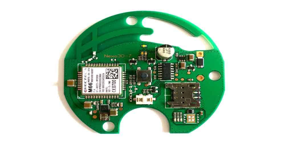
IoT PCB Design Components

The IoT Circuit boards are made up of a variety of parts. You need to comprehend these elements and their functions in this IoT system if you want to create IoT devices that work properly. The many types of IoT component are listed below:
Sensors
The sensor forms the initial part of the IOT PCB. A special function for sensors exists inside this IoT PCB system. Also, they perform crucial duties in this IoT system, including data and information collection. Although there are many various types of sensors utilized for IoT Boards, the most typical ones are a pressure sensor, temperature sensor, humidity sensor, camera, RFI tag, and IR sensor.
Wireless connectivity
The IoT PCB’s wireless connectivity provides efficient data exchange or communication between several sensors. Once data has been collected by the sensors, it is wirelessly sent to various layers of such IoT PCB to undergo additional processing. Z-wav Wifi, Zigbee, Bluetooth, Lora, NFC, and other widely used wireless technologies are incorporated onto IoT Boards.
System for managing power
The power control system is the third element of an IoT PCB. This system aids in controlling and managing power flow within your IoT PCB. Due to the continual connection between the various IoT device components and their network, particular consideration should be paid to the power supply of these devices to ensure longevity.
The PCB must be carefully built for any IoT device using batteries to ensure effective power utilization. Utilizing a voltage regulator with little quiescent power is one method to accomplish this.
The Importance of Size in the IoT PCB Design
The most important need for every IoT product is size. IoT PCB design must take physical constraints like size and flexibility into account.
Because IoT devices are constantly connected via a unique communication network, any related battery design requires power consumption optimization.
The internet-based data interchange between IoT devices is smooth. The user information must be safeguarded, and this design must adhere to security standards.
In order to earn and keep the public’s trust in IoT devices, reliability standards are rising as well to help build as well as maintain customer’s trust. Thus, thorough simulations and prototypes are needed for IoT PCB design.
Suggestions for Optimized IoT PCB Design
Apart from the planned arrangement of components, vias, and tracks, the tiny size constraint has not left any extra board space. Only Flex PCBs and HDI PCBs having features such as small connection pad, thick wiring, as well as miniatured vias may enable the functioning of the compact design.
The right component choice is essential to the IoT PCB design. It’s crucial to pick the right wireless modules, RF components, etc. because the application requires much internet access to ensure the gathering and analysis of sensitive data. During the process of component selection, the network speed and range of these components must be assessed.
Power management is vital for such prolonged battery demand in any IoT architecture. This demands for a stringent power budgeting for every circuit block. This is known that wireless transceivers experience significant energy absorptions throughout transitions. Their battery life is also influenced by the integrated circuits’ power needs when they are in sleep mode. Therefore, it is advised that the power needs be tested beforehand in the IoT PCB design.
Whenever it involves product fitting, IoT products include a variety of specifications. To easily incorporate your design into the chosen IoT product form, be sure to prototype it thoroughly. It is advised to model the mechanics of the design which could be impacted by the human contacts, such as body warmth, constant movement, or moisture, in the IoT designs intended for user wearables.
The thermal consequences of such items must be examined, and the circuit board design must provide an adequate cooling alternative. For low-space as well as high-efficiency requirements, choosing more recent packaging technologies including multi-chip modules or System-in-package is advised.
Benefits of IoT PCB Design
You might be asking why IoT PCB use is growing so quickly and becoming so popular. This can be attributed to the idea that they offer a number of benefits when used to various sectors. The following reveals just few out of the countless benefits of IoT PCBs:
Small size
The IoT PCB’s singular benefit is that it takes up small board space, providing it a compact dimension or form. It can because of the thin components employed in their manufacturing. This enables parts like satellites, batteries, and microphones to be fitted in compact spaces without compromising their functionality.
Lightweight
The entire weight of an IoT device is drastically reduced as a result of the modest size of the IoT PCB. As a result, IoT devices are incredibly light, an additional special benefit of contemporary technology. The majority of IoT devices come lightweight, portable, and even wearable. IoT PCBs are convenient for users of IoT devices due to their compact size and low weight.
Durability
In a variety of industries, IoT PCBs could survive challenging environmental conditions. They can continue operating in such hostile conditions without malfunctioning. In large part because of the HDI PCBs utilized in their manufacturing, IoT devices are extremely robust and able to withstand stress in challenging settings.
Easy wiring routes
IoT Boards feature straightforward wire connections and simple wiring paths. This makes it possible to avoid using complicated electrical and mechanical connectors and has a significant positive impact on IoT Boards by enhancing their functionality.
The Applications of the IoT PCB Design
IoT PCBs are widely used in many different industries. These can be applied to smart home products, cellphones, smartwatches, automotive dashboards, and other devices. These are a few more widely used IoT PCB applications.
- IoT PCBs are used by automotive sensors to improve convenience and performance.
- Color-changing light bulbs that can be controlled from tablets and even small smart devices to generate certain moods for various rooms.
- Grid designs in shopping malls or theme parks that track visitor paths to offer retailers and patrons specialized sale opportunities.
- GPS and satellite technologies
- Modules for fitness trackers
- IoT PCBs are used in digital trains for convenient time monitoring as well as transit.
- Medical equipment
- Modules for fitness trackers
- Smart agricultural system
Conclusion
Since so many consumer IoT applications operate at extremely high frequencies, its RF spectrum has become congested. Unwanted interference as well as safety concerns have resulted from this. IoT PCB design for safety application is crucial. To lessen the risks from EMI, PCB designers must provide shielding over sensitive electronics. An effective grounding system offers protection from interference problems.
