IR proximity sensors are used in a variety of applications, from robotics to security systems. These sensors work by emitting infrared light and measuring the reflection off of nearby objects. The PCB (printed circuit board) layout of an IR proximity sensor is crucial to its performance and accuracy.
The layout of an IR proximity sensor PCB can affect the sensor’s range, sensitivity, and noise level. Designers must consider the placement of the sensor, the size and shape of the PCB, and the routing of traces and components. Proper layout can help to minimize noise and interference, resulting in more accurate readings. In addition, a well-designed layout can help to optimize the sensor’s range and sensitivity, allowing it to detect objects at greater distances.
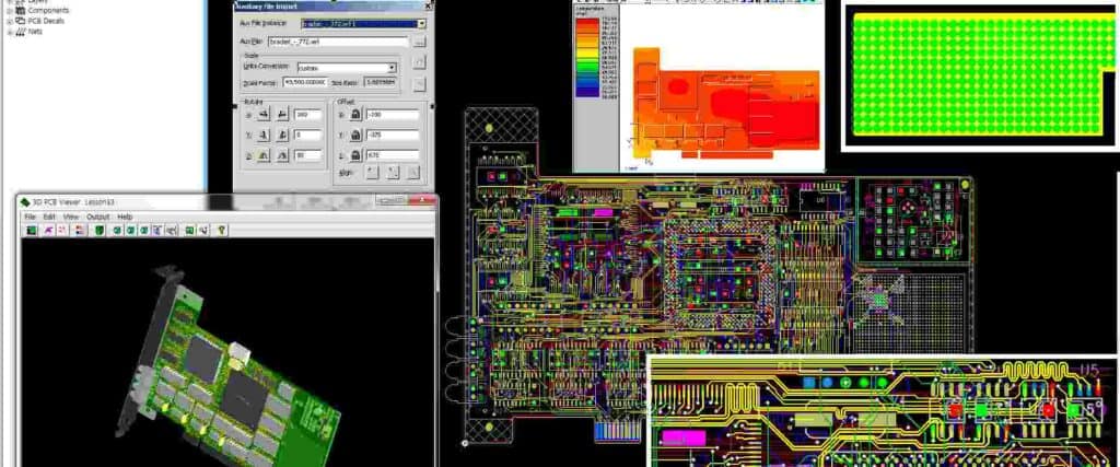
IR Proximity Sensor PCB Layout Design
When designing a printed circuit board (PCB) for an IR proximity sensor, there are several important considerations to keep in mind. Proper layout design can help ensure optimal performance and accuracy of the sensor.
Design Considerations
The layout of an IR proximity sensor PCB should take into account the following factors:
- Sensor placement: The IR sensor should be placed in a location that allows for accurate detection of the target object. This may require careful consideration of the sensor’s field of view and the desired sensing distance.
- Power supply: The sensor requires a stable power supply to function properly. The PCB layout should include a power supply circuit that minimizes noise and voltage fluctuations.
- Signal processing: The sensor’s output signal needs to be processed before it can be used. The PCB layout should include a signal processing circuit that filters and amplifies the sensor’s output signal.
Components Placement
When placing components on the PCB, it’s important to consider the following:
- Sensor placement: As mentioned earlier, the IR sensor should be placed in a location that allows for accurate detection of the target object.
- Power supply components: The power supply circuit should be placed as close to the sensor as possible to minimize noise and voltage fluctuations.
- Signal processing components: The signal processing circuit should be placed close to the sensor to minimize noise and signal degradation.
PCB Traces Routing
The routing of PCB traces can also affect the performance of the IR proximity sensor. Here are some guidelines to follow:
- Signal traces: The signal traces should be kept as short as possible to minimize noise and signal degradation.
- Power traces: The power traces should be wider than signal traces to minimize voltage drop and noise.
- Ground traces: The ground traces should be routed in a way that minimizes noise and interference.
By following these guidelines, you can design a PCB layout that maximizes the performance and accuracy of your IR proximity sensor.
Testing and Validation
Functional Testing
Before deployment, it is important to conduct functional testing of the IR proximity sensor PCB layout to ensure proper operation. This testing involves verifying that the sensor can detect objects at the desired distance and trigger the appropriate output signal.
To perform functional testing, a test setup can be created with a known object placed at a specific distance from the sensor. The sensor’s output signal can be monitored using an oscilloscope or a multimeter to ensure that it is working as expected.
Environmental Testing
Environmental testing is also an important part of validating the IR proximity sensor PCB layout. This testing involves subjecting the sensor to various environmental conditions to ensure that it can operate reliably in different situations.
Some common environmental factors to test include temperature, humidity, and vibration. The sensor should be tested at different temperature ranges to ensure that it can operate within specified limits. Humidity testing can help verify that the sensor can operate in high humidity environments without malfunctioning. Vibration testing can help ensure that the sensor can withstand mechanical stress without damage.
Overall, functional and environmental testing are critical steps in validating an IR proximity sensor PCB layout. By conducting these tests, designers can ensure that the sensor will operate reliably in a variety of situations, giving users confidence in its performance.
Manufacturing and Assembly

PCB Fabrication
The PCB layout for an IR proximity sensor is a critical component of the overall design. The PCB should be designed with the specific requirements of the sensor in mind, including the size, shape, and placement of the components. The layout should also consider the manufacturing process, as this can impact the final performance of the sensor.
When manufacturing the PCB, it is important to select a reliable and experienced PCB fabrication company. The company should have experience with IR proximity sensors and be able to produce high-quality PCBs with tight tolerances. The fabrication company should also be able to provide guidance on the best materials and manufacturing processes for the specific design.
Component Sourcing
The components used in the IR proximity sensor should be carefully selected to ensure optimal performance. It is important to source components from reputable suppliers that can provide high-quality components with consistent performance. The components should also be compatible with the manufacturing process and the PCB layout.
When sourcing components, it is important to consider the lead time and availability of the components. It is also important to consider the cost of the components and the overall budget for the project.
Assembly Process
The assembly process for the IR proximity sensor should be carefully planned and executed to ensure optimal performance. The assembly process should be designed to minimize the risk of errors and defects, while also ensuring that the components are properly aligned and secured.
During the assembly process, it is important to follow the manufacturer’s guidelines and best practices. This includes using the correct tools and equipment, as well as following the recommended soldering techniques. It is also important to test the sensor after assembly to ensure that it is functioning properly.
Overall, the manufacturing and assembly process for an IR proximity sensor requires careful planning, attention to detail, and a commitment to quality. By following best practices and working with experienced suppliers and manufacturers, it is possible to produce a high-quality sensor that meets the specific requirements of the design.
