Keyboard PCB design is a crucial aspect of building a custom keyboard. PCBs, or printed circuit boards, connect the various components of a keyboard, such as switches and LEDs, and allow them to communicate with each other. One popular software for designing keyboard PCBs is KiCad.
KiCad is an open-source software that allows users to design schematics, layout PCBs, and generate Gerber files for manufacturing. It has gained popularity among keyboard enthusiasts due to its user-friendly interface and powerful features, such as 3D visualization of the PCB layout. Additionally, KiCad has a large community of users who have created libraries of components and shared their designs, making it easier for newcomers to get started.
What is a Keyboard PCB?
Definition
A Keyboard PCB, or Printed Circuit Board, is a vital component in the construction of a mechanical keyboard. It is a thin board made of fiberglass or other composite material, with copper traces etched onto it. These traces serve as pathways for the electrical signals that control the keyboard’s switches and LEDs.
Function
The main function of a Keyboard PCB is to provide a stable and reliable platform for the switches and other components that make up the keyboard. It also acts as a hub for all the electrical signals that flow through the keyboard, ensuring that they are properly routed and processed.
A well-designed Keyboard PCB can make a big difference in the performance and feel of a mechanical keyboard. It can allow for more efficient and accurate typing, reduce latency and input lag, and even provide advanced features such as programmable macros and RGB lighting.
In summary, a Keyboard PCB is a crucial component in the construction of a mechanical keyboard, providing a stable and reliable platform for the switches and other components, and ensuring that the electrical signals are properly routed and processed.
Why Use KiCad for Keyboard PCB Design?
Advantages of KiCad
KiCad is an open-source software that is available for free. This means that users can access all of its features without having to pay any licensing fees. Additionally, KiCad is constantly being updated and improved by a community of developers, which means that users can benefit from new features and bug fixes as soon as they are released.
Another advantage of KiCad is that it is highly customizable. Users can modify the software to suit their specific needs and preferences. This includes creating custom libraries, templates, and scripts. Users can also create their own plugins to extend the functionality of the software.
Features of KiCad
KiCad offers a range of features that make it an ideal choice for keyboard PCB design. One of the most important features is the ability to create custom footprints and symbols. This means that users can create unique designs that are tailored to their specific requirements.
KiCad also offers a range of tools for schematic capture and PCB layout. These tools are easy to use and allow users to create complex designs quickly and efficiently. The software also includes a 3D viewer that allows users to visualize their designs in three dimensions.
Another important feature of KiCad is its ability to generate Gerber files. Gerber files are used to manufacture PCBs, and KiCad can generate these files automatically. This means that users can quickly and easily send their designs to a manufacturer without having to worry about file compatibility issues.
Overall, KiCad is an excellent choice for keyboard PCB design. Its open-source nature, customizability, and range of features make it a powerful and flexible tool for any designer.
Designing a Keyboard PCB in KiCad

Creating a New Project
To design a keyboard PCB in KiCad, the first step is to create a new project. Open KiCad and select “File” > “New Project” > “New Project.” Give your project a name and select a location to save it. Then, select “PCB Layout” as the project type and “Use existing footprint libraries” as the footprint libraries option.
Schematic Design
Once you have created your project, the next step is to design the schematic. Click on “Schematic Editor” in the project window to open the schematic editor. Here, you can add components to your schematic by selecting them from the libraries and placing them on the schematic sheet. Connect the components by adding wires and labels.
PCB Layout Design
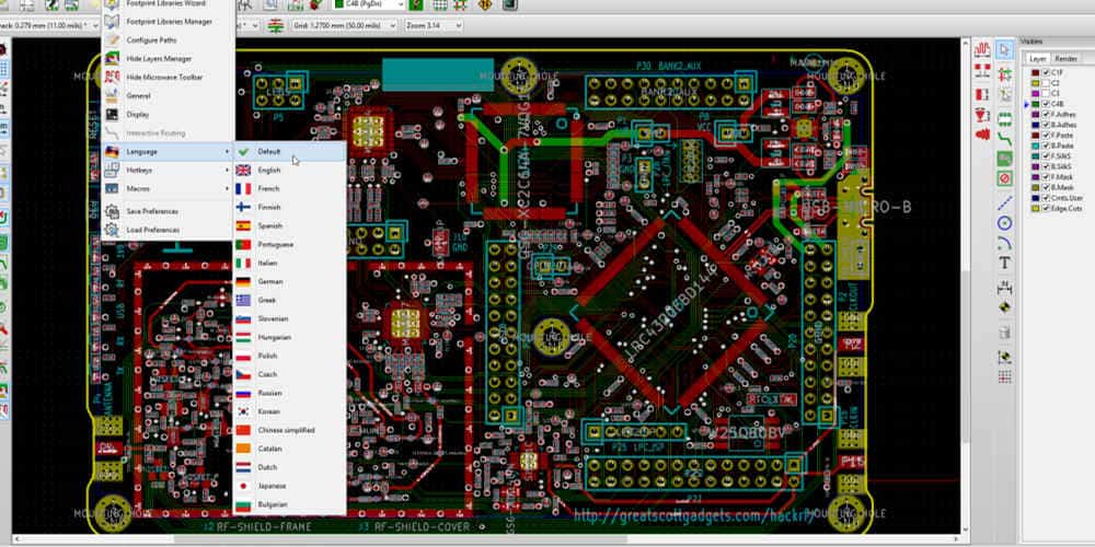
After designing the schematic, the next step is to create the PCB layout. Click on “PCB Layout Editor” in the project window to open the PCB editor. Here, you can place the components on the PCB board and route the connections between them. Use the “Add Tracks and Vias” tool to add traces and vias to the board. You can also use the “Design Rules” tool to set up design rules for your PCB layout.
Generating Gerber Files
Once you have completed the PCB layout design, the final step is to generate the Gerber files. Go to “File” > “Plot” to open the plot dialog. Here, you can select the layers you want to plot and set up the plot parameters. After that, click on “Plot” to generate the Gerber files. You can then use these files to manufacture your keyboard PCB.
In summary, designing a keyboard PCB in KiCad involves creating a new project, designing the schematic, designing the PCB layout, and generating the Gerber files. With KiCad’s powerful tools and features, you can create high-quality and professional-grade PCB designs for your keyboard projects.
Keyboard PCB Components
When designing a keyboard PCB in KiCad, there are several important components to consider. These components include the microcontroller, switches, diodes, and LEDs.
Microcontroller
The microcontroller is the brain of the keyboard PCB. It is responsible for processing the key presses and sending the corresponding signals to the computer. Some popular microcontrollers used in keyboard PCBs include the Atmel AVR, Teensy, and STM32.
When selecting a microcontroller, it is important to consider factors such as the number of pins required, the amount of memory needed, and the programming language used. Additionally, some microcontrollers may require additional components such as voltage regulators or crystal oscillators.
Switches
Switches are the physical components that are pressed to register a key press. There are various types of switches available, including mechanical, membrane, and capacitive switches. Mechanical switches are the most popular type of switch used in keyboard PCBs due to their tactile feedback and durability.
When selecting switches, it is important to consider factors such as the actuation force, travel distance, and switch type. Some popular switch brands include Cherry MX, Gateron, and Kailh.
Diodes
Diodes are used in keyboard PCBs to prevent ghosting and ensure that only one key press is registered at a time. Each switch requires a diode to be placed in series with it. The most commonly used diodes in keyboard PCBs are 1N4148 and 1N4148W.
LEDs
LEDs can be used to add backlighting or underglow to a keyboard PCB. When selecting LEDs, it is important to consider factors such as the size, color, and brightness. Additionally, resistors may be required to ensure that the LEDs do not draw too much current.
In conclusion, when designing a keyboard PCB in KiCad, it is important to carefully consider the microcontroller, switches, diodes, and LEDs. By selecting the appropriate components, you can create a keyboard that is both functional and aesthetically pleasing.
Tips for Designing a Successful Keyboard PCB

Consider the Layout and Ergonomics
When designing a keyboard PCB, it’s important to consider the layout and ergonomics of the keyboard. The layout should be intuitive and easy to use, with keys in the right places for the user’s needs. Ergonomics should also be taken into account, with the keyboard designed to be comfortable and easy to use for extended periods of time.
One important factor to consider is the placement of the keys. The most frequently used keys should be placed in the most accessible locations, while less frequently used keys should be placed in less accessible locations. This will help to reduce strain on the user’s hands and fingers, and make typing more comfortable.
Test and Iterate
It’s important to test and iterate your keyboard PCB design to ensure that it meets your requirements. This can be done by creating prototypes and testing them out in real-world scenarios. By testing and iterating your design, you can identify any issues or areas for improvement, and refine your design accordingly.
One useful tool for testing your keyboard PCB design is a keyboard tester. This will allow you to test the functionality of your keyboard and identify any issues with the layout or key placement.
Use High-Quality Components
When designing a keyboard PCB, it’s important to use high-quality components. This will ensure that your keyboard is reliable and long-lasting, and that it performs well over time. High-quality components will also help to reduce the risk of failures or malfunctions, and ensure that your keyboard is safe to use.
Some key components to consider when designing your keyboard PCB include switches, diodes, and capacitors. These components should be selected based on their quality, durability, and performance characteristics, and should be sourced from reputable manufacturers.
In conclusion, designing a successful keyboard PCB requires careful consideration of the layout and ergonomics, testing and iteration, and the use of high-quality components. By following these tips, you can create a keyboard that is comfortable, reliable, and easy to use.
