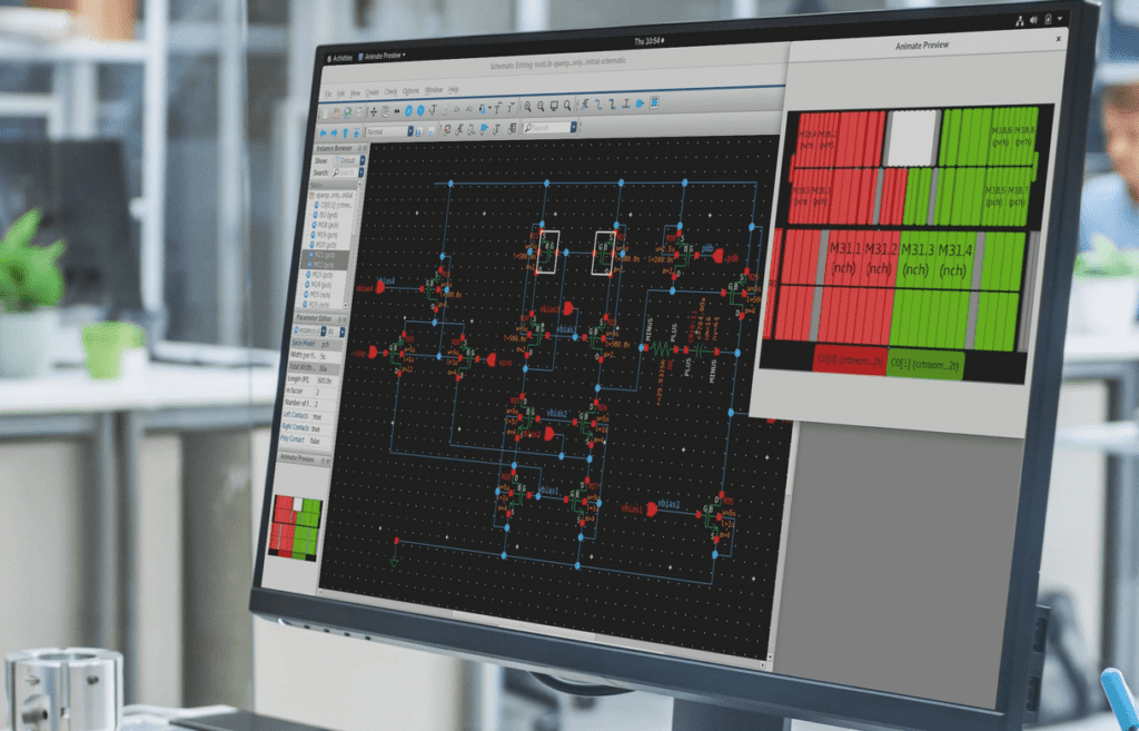
Layout PCB final is an essential process that involves the placement of electronic components on a printed circuit board (PCB). It is the final step in the PCB design process, where the designer ensures that all the components are arranged in the most optimal way possible. The layout PCB final process involves various stages, including component placement, routing, and signal integrity checks.
During the layout PCB final process, the designer must take into consideration various factors such as the size and shape of the PCB, the number of components, and the intended function of the circuit. The designer must also ensure that the components are placed in a way that allows for efficient routing of traces and minimal signal interference. Additionally, the designer must ensure that the PCB layout meets industry standards and regulations, and is manufacturable within the given budget and time constraints.
Preparing for PCB Layout Final
Reviewing Design Requirements
Before starting the final PCB layout, it is essential to review the design requirements. This involves checking the schematic and verifying that all the components are correctly placed and connected. It is also crucial to ensure that all the design requirements, such as signal integrity, power distribution, and thermal management, are met.
Identifying Components and Placement
The next step is to identify all the components and their placement on the PCB. This includes determining the size, shape, and orientation of each component to ensure that they fit together correctly. It is also important to consider the placement of critical components, such as power supplies, connectors, and high-speed signal paths, to minimize noise and interference.
Establishing Design Rules
Once the components are identified, the next step is to establish the design rules. This includes defining the minimum trace width, spacing, and clearance, as well as the via size and placement. It is also important to establish the design rules for power planes, ground planes, and signal layers to ensure that the PCB meets the design requirements.
Routing Strategies
The final step is to determine the routing strategies. This involves deciding on the routing order, the layer stackup, and the routing topology. It is also important to consider the routing length and impedance matching for high-speed signals. The routing strategies should be optimized to minimize noise, crosstalk, and signal loss.
In conclusion, preparing for PCB layout final involves reviewing the design requirements, identifying components and placement, establishing design rules, and determining routing strategies. By following these steps, the final PCB layout can be optimized to meet the design requirements, minimize noise and interference, and ensure signal integrity.
Executing PCB Layout Final

Creating the Board Outline
The first step in executing the final PCB layout is to create the board outline. This is done by drawing a rectangle or any other shape that represents the dimensions of the PCB. The board outline should be large enough to accommodate all the components and traces required for the circuit.
Placing Components
After creating the board outline, the next step is to place the components on the board. Components should be placed in a logical and organized manner, taking into consideration the signal flow and the physical constraints of the board. It is important to ensure that there is enough space between components to allow for easy routing of traces.
Routing Traces
Once the components are placed, the next step is to route the traces. Traces should be routed in a way that minimizes noise and interference. This can be achieved by routing high-speed signals first, followed by low-speed signals. It is also important to ensure that traces do not cross each other unnecessarily, as this can cause crosstalk and other signal integrity issues.
Adding Copper Pour Areas
Copper pour areas can be added to the PCB layout to provide a ground plane or power plane. This can help reduce noise and improve signal integrity. Copper pour areas should be placed strategically, taking into consideration the location of components and traces.
Adding Text and Graphics
Finally, text and graphics can be added to the PCB layout to provide additional information about the circuit. This can include component labels, reference designators, and other annotations. Graphics can also be added to make the layout more visually appealing and easier to understand.
In conclusion, executing the final PCB layout involves creating the board outline, placing components, routing traces, adding copper pour areas, and adding text and graphics. By following these steps, you can create a high-quality PCB layout that meets all the requirements of your circuit.
Verifying PCB Layout Final
Design Rule Check (DRC)
Before sending a PCB design for manufacturing, it is essential to run a Design Rule Check (DRC) to ensure that the layout meets the design requirements. A DRC compares the layout against a set of pre-defined design rules to ensure that the design is manufacturable.
The DRC process checks for issues such as spacing violations, trace widths, and drill sizes. It also checks for issues such as silkscreen text and pad placement. Running a DRC is critical to ensure that the PCB design is manufacturable and meets the design requirements.
Electrical Rule Check (ERC)
An Electrical Rule Check (ERC) is another essential step in verifying the PCB layout final. An ERC checks the electrical connectivity of the design to ensure that there are no electrical errors in the layout.
The ERC process checks for issues such as unconnected nets, incorrect pin assignments, and incorrect net names. An ERC is critical to ensure that the PCB design meets the electrical requirements and is free from electrical errors.
Signal Integrity Analysis
Signal Integrity (SI) analysis is a critical step in verifying the PCB layout final. SI analysis checks for issues such as signal reflections, crosstalk, and timing violations.
SI analysis ensures that the PCB design meets the signal quality requirements and is free from signal integrity issues. It is essential to perform SI analysis to ensure that the design meets the electrical requirements and is free from signal integrity issues.
Thermal Analysis
Thermal analysis is another critical step in verifying the PCB layout final. Thermal analysis checks for issues such as thermal hotspots, thermal gradients, and thermal stress.
Thermal analysis ensures that the PCB design meets the thermal requirements and is free from thermal issues. It is essential to perform thermal analysis to ensure that the design meets the thermal requirements and is free from thermal issues.
In conclusion, verifying the PCB layout final is a critical step in ensuring that the design is manufacturable, meets the design requirements, and is free from electrical, signal integrity, and thermal issues. By performing a DRC, ERC, SI analysis, and thermal analysis, designers can ensure that the PCB design meets all the requirements and is ready for manufacturing.
Preparing for PCB Fabrication
Before sending your PCB design to the manufacturer, it is important to prepare the necessary files for fabrication. This includes exporting Gerber files, generating drill files, and generating assembly files.
Exporting Gerber Files
Gerber files are the standard format used by PCB manufacturers to fabricate the layers of the board. To export Gerber files from your PCB design software, follow these steps:
- Open your PCB design software and select the “File” menu.
- Choose the “Export” option and select “Gerber” from the list of available formats.
- Verify that all necessary layers are selected for export, including copper layers, silkscreen layers, and solder mask layers.
- Save the Gerber files to a folder on your computer.
Generating Drill Files
Drill files are used to create the holes in your PCB. To generate drill files from your PCB design software, follow these steps:
- Open your PCB design software and select the “File” menu.
- Choose the “Export” option and select “Drill” from the list of available formats.
- Verify that all necessary layers are selected for export, including drill holes and tooling holes.
- Save the drill files to the same folder as the Gerber files.
Generating Assembly Files
Assembly files are used to show the manufacturer where to place components on your PCB. To generate assembly files from your PCB design software, follow these steps:
- Open your PCB design software and select the “File” menu.
- Choose the “Export” option and select “Assembly” from the list of available formats.
- Verify that all necessary layers are selected for export, including component outlines and reference designators.
- Save the assembly files to the same folder as the Gerber and drill files.
By following these steps, you can ensure that your PCB design is properly prepared for fabrication.
Conclusion
In conclusion, the layout PCB final is a crucial step in the PCB design process. It can make or break the functionality and reliability of the final product. Therefore, it is essential to pay attention to every detail during this stage.
To ensure the success of the final layout, it is important to follow best practices and guidelines. These include keeping the traces as short and direct as possible, avoiding crossing traces, and placing components in a logical and organized manner.
Additionally, it is critical to perform thorough testing and analysis of the final layout. This includes checking for signal integrity issues, power delivery problems, and thermal management concerns.
Overall, by following these guidelines and best practices, you can create a high-quality and reliable PCB layout that meets the requirements of your design.
