Low pass filter PCB layout is an essential aspect of electronic circuit design that is often overlooked. A low pass filter is a type of electronic filter that allows low-frequency signals to pass through while attenuating high-frequency signals. It is a fundamental component in electronic circuits used to eliminate unwanted noise and interference from signals.
To achieve the desired performance of a low pass filter, it is essential to consider its PCB layout. The layout of a low pass filter PCB can significantly affect its performance, including its frequency response, insertion loss, and phase shift. A poorly designed PCB layout can lead to unwanted crosstalk, parasitic capacitance, and inductance, which can adversely affect the filter’s performance. Therefore, it is crucial to understand the best practices for designing a low pass filter PCB layout to achieve optimal performance.
Basics of Low Pass Filter PCB Layout
What is a Low Pass Filter PCB Layout?
A low pass filter is an electronic circuit that allows low frequency signals to pass through while blocking high frequency signals. In a PCB layout, a low pass filter is designed to reduce high frequency noise and interference from the power supply or other sources. The low pass filter PCB layout consists of a series of capacitors and inductors arranged in a specific configuration to achieve the desired filtering effect.
Why is Low Pass Filter PCB Layout Important?
Low pass filter PCB layout is crucial for ensuring the proper functioning of electronic circuits. High frequency noise and interference can cause errors, malfunctions, and even damage to electronic components. By using a low pass filter PCB layout, the unwanted high frequency signals are removed, allowing the desired low frequency signals to pass through.
Factors to Consider in Low Pass Filter PCB Layout
When designing a low pass filter PCB layout, there are several factors to consider:
-
Component selection: Choosing the right capacitors and inductors is critical for achieving the desired filtering effect. The values of the components must be carefully selected based on the frequency range of the signals to be filtered.
-
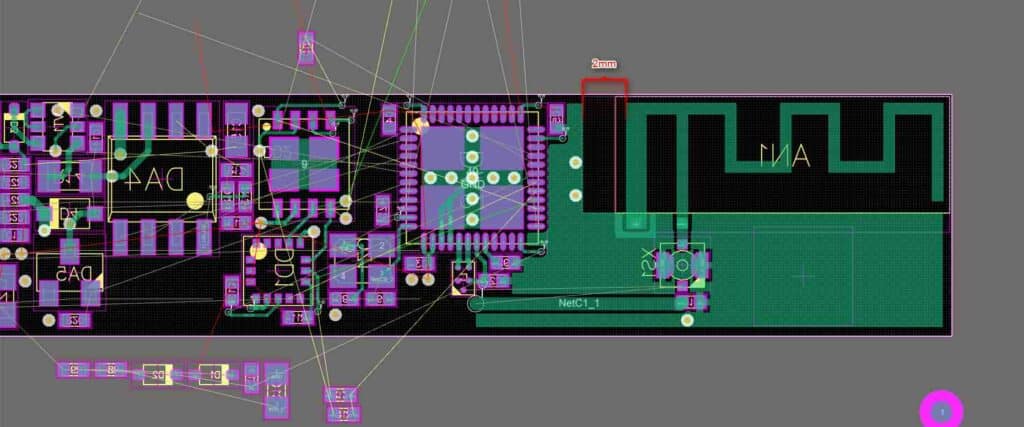
Placement: The placement of the components on the PCB can affect the performance of the low pass filter. The components should be placed as close as possible to the input and output terminals to minimize the length of the traces and reduce the risk of interference.
-
Trace routing: The traces that connect the components should be routed carefully to minimize the length and avoid crossing other traces or components that could cause interference.
-
Grounding: Proper grounding is essential for the proper functioning of the low pass filter. The ground plane should be connected to the input and output terminals of the filter, and the components should be grounded as close as possible to the ground plane.
By considering these factors, a well-designed low pass filter PCB layout can effectively reduce high frequency noise and interference, ensuring the proper functioning of electronic circuits.
Designing a Low Pass Filter PCB Layout

Steps to Design a Low Pass Filter PCB Layout
Designing a low pass filter PCB layout involves the following steps:
- Determine the cut-off frequency of the filter.
- Choose the appropriate filter topology.
- Select the components for the filter.
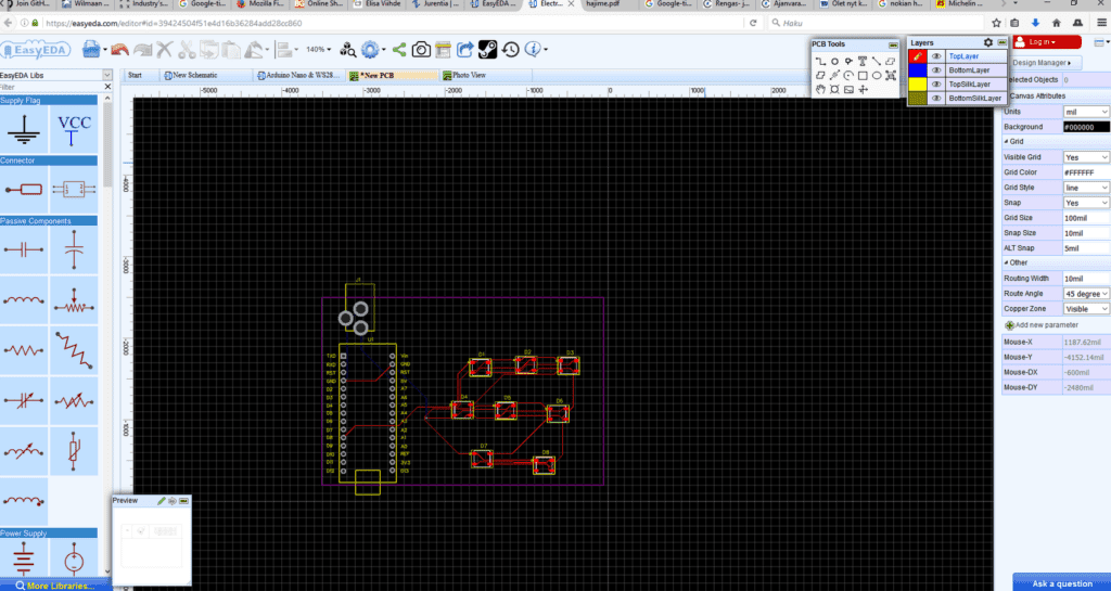
- Determine the PCB layout.
- Place the components on the PCB.
- Route the PCB traces.
- Verify the design using simulation software.
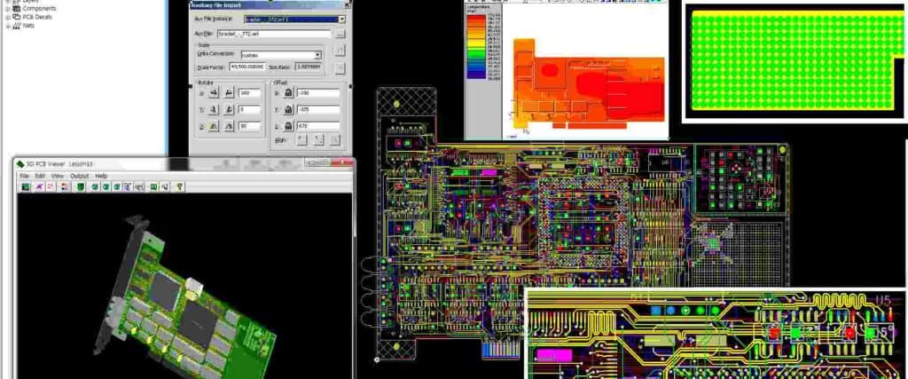
Tools for Designing a Low Pass Filter PCB Layout
The following tools are commonly used for designing a low pass filter PCB layout:
- Circuit simulation software, such as LTSpice or PSpice.
- PCB design software, such as Altium Designer or Eagle PCB.
- Signal generator and oscilloscope for testing the filter.
When designing a low pass filter PCB layout, it is important to consider the location and orientation of components, as well as the routing of traces to minimize noise and interference. The use of ground planes and shielding can also help improve the performance of the filter.
In conclusion, designing a low pass filter PCB layout requires careful consideration of the filter topology, component selection, and PCB layout. With the right tools and techniques, it is possible to create a high-performance filter that meets the desired specifications.
Best Practices for Low Pass Filter PCB Layout
Placement of Components
The placement of components in a low pass filter PCB layout is critical to achieving optimal performance. It is recommended to place the inductors and capacitors as close as possible to each other, and to the input and output pins of the filter. This helps to minimize the parasitic effects of the traces and reduce the overall size of the filter.
Routing of Traces
The routing of traces in a low pass filter PCB layout is also crucial. It is recommended to keep the traces as short as possible, and to avoid sharp bends and corners. This helps to minimize the parasitic effects of the traces and reduce the overall size of the filter. Additionally, it is recommended to use wider traces to reduce the resistance and inductance of the traces.
Ground Planes
Ground planes are an important aspect of low pass filter PCB layout. It is recommended to use a solid ground plane to minimize the parasitic effects of the traces and reduce the overall size of the filter. Additionally, it is recommended to connect the ground plane to the input and output pins of the filter, as well as to the ground of the rest of the circuit.
Decoupling Capacitors
Decoupling capacitors are essential for low pass filter PCB layout. It is recommended to place decoupling capacitors as close as possible to the power supply pins of the filter. This helps to reduce the noise and ripple on the power supply, which can affect the performance of the filter.
In summary, the placement of components, routing of traces, ground planes, and decoupling capacitors are all important aspects of low pass filter PCB layout. By following these best practices, it is possible to achieve optimal performance and reduce the overall size of the filter.
Common Mistakes in Low Pass Filter PCB Layout
Incorrect Component Placement
One of the most common mistakes in low pass filter PCB layout is incorrect component placement. This can result in poor filter performance or even complete failure. Components should be placed as close as possible to each other and in the correct orientation. Make sure to follow the manufacturer’s recommended layout guidelines for each component.
Improper Trace Routing
Another common mistake is improper trace routing. The traces should be short and direct, avoiding any sharp turns or kinks. The width of the traces should also be appropriate for the current they will be carrying. The use of vias should be minimized, as they can cause additional losses and impedance mismatches.
Inadequate Ground Planes
Inadequate ground planes can also cause problems in low pass filter PCB layout. A solid ground plane should be used for the entire circuit, with vias connecting the top and bottom layers. The ground plane should be as large as possible and should be placed directly under the signal traces. Make sure to avoid any gaps or voids in the ground plane, as they can cause unwanted resonances and noise.
By avoiding these common mistakes, you can ensure that your low pass filter PCB layout is optimized for performance and reliability.
Conclusion
Designing a low pass filter PCB layout can be a challenging task, but it is essential for ensuring the proper functioning of electronic circuits. In this article, we have discussed the key considerations for designing a low pass filter PCB layout, including the selection of components, the placement of components, and the routing of traces.
When designing a low pass filter PCB layout, it is crucial to consider the frequency range of the filter, as well as the desired attenuation level. The selection of appropriate components, such as capacitors and inductors, is critical for achieving the desired filter characteristics.
Additionally, the placement of components on the PCB can have a significant impact on the performance of the filter. Placing components too closely together can result in unwanted coupling and interference, while placing them too far apart can increase the overall size of the PCB.
Finally, the routing of traces is another critical consideration for designing a low pass filter PCB layout. Traces should be kept as short as possible to minimize signal loss and interference, and they should be routed in a way that minimizes crosstalk and interference between different components.
Overall, designing a low pass filter PCB layout requires careful consideration of a variety of factors, including component selection, placement, and routing. By following the guidelines outlined in this article, designers can create effective low pass filter PCB layouts that meet the requirements of their specific applications.
