Table of Contents
ToggleMixed signal PCB layout refers to the process of designing and implementing printed circuit boards that contain both analog and digital components. These components operate at different frequencies and have different signal requirements, which can introduce challenges when designing a layout that maintains signal integrity. The goal of mixed signal PCB layout is to minimize noise, crosstalk, and other sources of interference that can degrade the performance of the circuit.
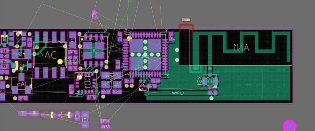
When designing a mixed signal PCB, it is important to consider the placement and routing of components, as well as the ground and power planes. The placement of components can affect the performance of the circuit by introducing unwanted noise or crosstalk. Routing signals on the PCB also requires careful consideration, as the length and placement of traces can impact signal integrity. Ground and power planes are also important, as they provide a low-impedance path for signals and help to reduce noise and interference.
Overall, mixed signal PCB layout is a complex process that requires careful planning and consideration of various factors. By following best practices and utilizing specialized design tools, designers can create layouts that minimize noise and interference, and ensure optimal performance of their mixed signal circuits.

Mixed Signal PCB Layout Design Considerations
When designing a mixed signal PCB, there are several considerations that need to be taken into account to ensure that the analog and digital signals do not interfere with each other.
Ground Planes
Ground planes are a crucial aspect of mixed signal PCB layout design. Separating the analog and digital ground planes is essential to prevent noise interference. The ground planes should be connected at a single point to avoid ground loops. Additionally, the ground planes should be routed in a way that minimizes the loop area and reduces the risk of electromagnetic interference (EMI).
Component Placement
The placement of components is also critical in mixed signal PCB layout design. The analog and digital components should be separated as much as possible to avoid interference. The analog components should be placed on one side of the board, and the digital components on the other side. This helps to prevent digital noise from affecting the analog circuits.
Signal Routing
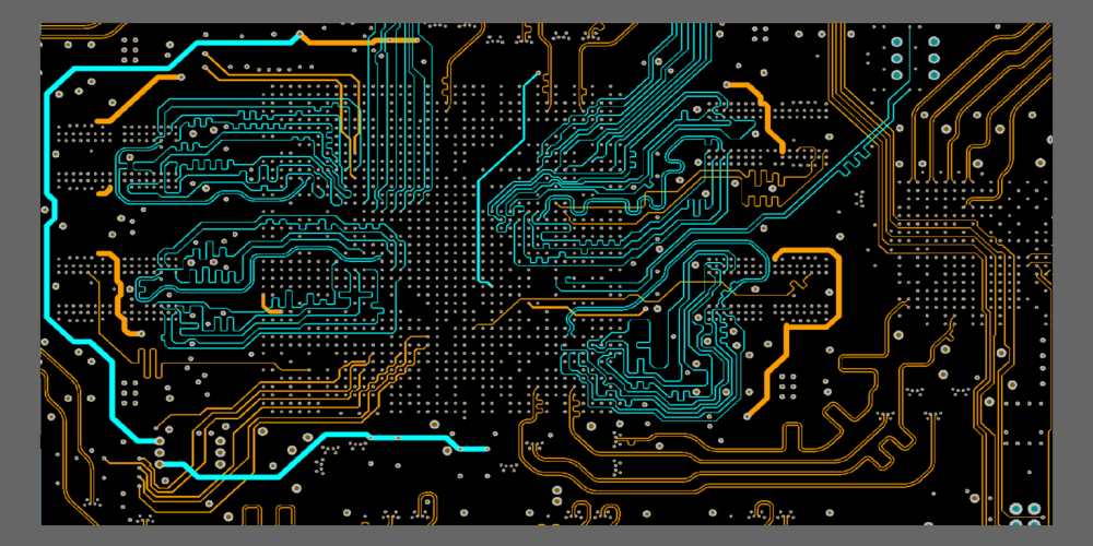
The routing of signals is another important consideration in mixed signal PCB layout design. The analog and digital signals should be routed separately to minimize crosstalk. Crosstalk occurs when a signal from one circuit interferes with the signal in another circuit. To prevent crosstalk, the analog and digital signals should be routed perpendicular to each other.
Power Supply
The power supply is also an essential consideration in mixed signal PCB layout design. The analog and digital power supplies should be separated to prevent noise interference. The power supply decoupling capacitors should be placed as close as possible to the components they are intended to serve.
In summary, designing a mixed signal PCB requires careful consideration of ground planes, component placement, signal routing, and power supply. By following these design considerations, it is possible to minimize noise interference and ensure that the analog and digital circuits operate independently.
Mixed Signal PCB Layout Techniques

Mixed signal PCB layout is a critical aspect of electronic design that involves combining analog and digital circuitry on the same board. The goal of mixed signal PCB layout is to minimize noise, crosstalk, and other signal integrity issues that can arise when analog and digital signals interact with each other.
To achieve this goal, there are several techniques that designers can use when laying out mixed signal PCBs. Some of the most important techniques include:
-
Separating Analog and Digital Ground Planes: One of the most effective ways to reduce noise and crosstalk is to use separate ground planes for analog and digital circuits. This helps to prevent digital noise from interfering with sensitive analog signals.
-
Star Grounding: Another technique for reducing noise is to use a star grounding scheme. This involves connecting all ground points to a single point, which can reduce ground loops and other sources of noise.
-
Signal Isolation: When designing mixed signal PCBs, it’s important to isolate analog and digital signals from each other as much as possible. This can be achieved using techniques such as differential signaling, shielding, and filtering.
-
Component Placement: The placement of components on the PCB can also have a significant impact on signal integrity. For example, placing analog and digital components on opposite sides of the board can help to reduce crosstalk.
-
Trace Routing: Proper trace routing is critical for minimizing noise and crosstalk. Some important considerations include keeping traces as short as possible, avoiding sharp angles, and using ground planes to shield sensitive signals.
By using these techniques and others, designers can create mixed signal PCB layouts that are optimized for signal integrity and performance.
Mixed Signal PCB Layout Best Practices

When designing a mixed signal PCB, it is important to follow certain best practices to minimize noise and interference. Here are some tips to keep in mind:
-
Separate Analog and Digital Ground Planes: Analog and digital circuits should have their own separate ground planes to prevent noise from being introduced into the analog circuitry. These ground planes should be connected at a single point to prevent ground loops.
-
Keep Analog and Digital Components Separate: Analog and digital components should be placed on separate areas of the PCB to prevent interference. If it is not possible to keep them completely separate, they should be placed as far apart from each other as possible.
-
Use Decoupling Capacitors: Decoupling capacitors should be placed as close as possible to the power pins of all ICs to filter out high-frequency noise. Capacitors with a low equivalent series resistance (ESR) and a high capacitance value are ideal for this purpose.
-
Route Analog and Digital Signals Separately: Analog and digital signals should be routed on separate signal layers of the PCB to prevent crosstalk. If it is not possible to route them separately, they should be routed perpendicular to each other.
-
Minimize Trace Lengths: Longer trace lengths can introduce more noise and interference. Try to keep trace lengths as short as possible, especially for high-frequency signals.
By following these best practices, you can design a mixed signal PCB that is less susceptible to noise and interference, resulting in better overall performance.

