Table of Contents
ToggleFusion 360 is a powerful software tool that can be used for printed circuit board (PCB) design. PCBs are essential components in modern electronics, and designing them correctly is crucial for ensuring proper functionality. Fusion 360’s PCB design capabilities can simplify the design process and help users create high-quality PCBs.
One of the key advantages of using Fusion 360 for PCB design is its integration with other design tools. Users can easily import 3D models and incorporate them into their PCB designs, which can be especially useful for designing enclosures or other components that need to fit together precisely. Fusion 360 also offers a range of simulation tools that can help users test their designs and identify potential issues before manufacturing.
Another benefit of using Fusion 360 for PCB design is its user-friendly interface. The software is designed to be intuitive and easy to use, even for those who are new to PCB design. This can help users save time and avoid frustration, allowing them to focus on creating the best possible PCB designs.

Overview
In this article, we will discuss PCB design with Fusion 360. We will cover the basics of PCB design, what Fusion 360 is, and why it is a great tool for PCB design.
What is PCB Design?
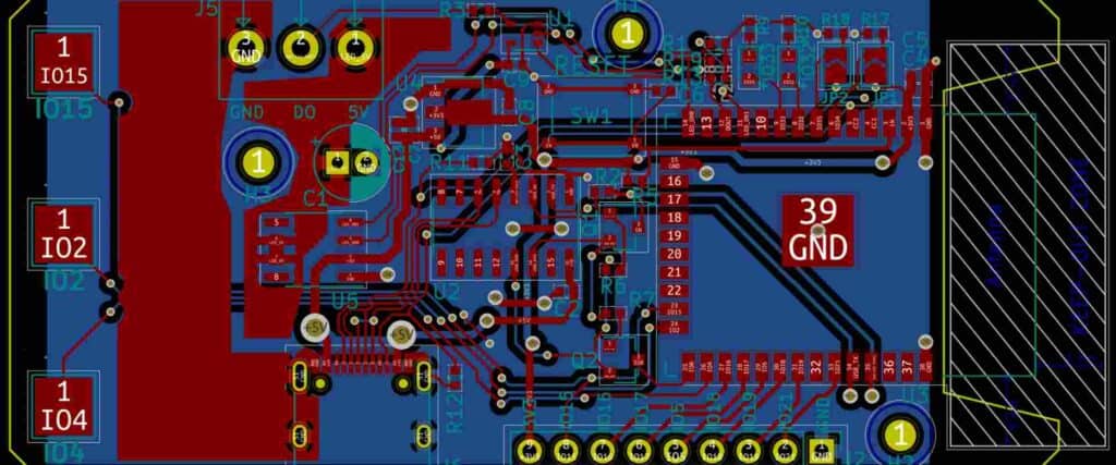
PCB design is the process of creating a printed circuit board (PCB) that connects electronic components. PCB design involves creating a schematic diagram of the circuit, placing the components on the board, and routing the electrical connections between them. PCBs are used in a wide variety of electronic devices, from smartphones to industrial machinery.
What is Fusion 360?
Fusion 360 is a cloud-based 3D CAD/CAM tool that provides a complete solution for product design and manufacturing. Fusion 360 is designed to be easy to use, yet powerful enough to handle complex design projects. It includes a wide range of tools for 3D modeling, simulation, and visualization, as well as tools for creating 2D drawings and schematics.
Why Use Fusion 360 for PCB Design?
Fusion 360 is an excellent tool for PCB design for several reasons:
- Integration: Fusion 360 integrates seamlessly with other CAD and PCB design tools, making it easy to import and export designs.
- Collaboration: Fusion 360 is a cloud-based tool that allows multiple users to work on the same project simultaneously, making it easy to collaborate with team members and clients.
- Simulation: Fusion 360 includes simulation tools that allow you to test your PCB design virtually before manufacturing, saving time and money.
- Manufacturing: Fusion 360 includes tools for CAM (computer-aided manufacturing) that allow you to generate toolpaths for CNC machines, making it easy to manufacture your PCB design.
Overall, Fusion 360 is a powerful, easy-to-use tool that is well-suited for PCB design.
Getting Started

If you’re new to PCB design with Fusion 360, this section will help you get started. We’ll walk you through the process of creating a new PCB design project, setting up the workspace, adding components, creating the schematic, and generating the PCB layout.
Creating a New PCB Design Project
To create a new PCB design project in Fusion 360, follow these steps:
- Open Fusion 360 and click on the “File” menu.
- Select “New Design” and choose “PCB Design” from the dropdown menu.
- Choose the units you want to use for your design and click “OK”.
Setting Up the Workspace
After creating a new PCB design project, you’ll need to set up the workspace to start designing. Here’s how:
- Click on the “PCB” button in the toolbar to switch to the PCB workspace.
- Choose the “Schematic” tab and click on “New Schematic”.
- Choose the “PCB” tab and click on “New Board”.
Adding Components
To add components to your PCB design, follow these steps:
- Go to the “Components” panel and click on “Add Component”.
- Search for the component you want to add and select it from the list.
- Place the component on the schematic or board by clicking on the location.
Creating the Schematic
To create the schematic for your PCB design, follow these steps:
- Add components to the schematic as described in the previous section.
- Connect the components by clicking on the “Wire” button in the toolbar and drawing wires between the pins.
- Add labels and annotations to the schematic to make it clear and easy to understand.
Generating the PCB Layout
After creating the schematic, you can generate the PCB layout. Here’s how:
- Click on the “PCB Layout” button in the toolbar to switch to the PCB layout workspace.
- Choose the “From Schematic” option and click on “Create PCB”.
- Adjust the placement and routing of the components to optimize the layout.
That’s it! You’ve now learned the basics of getting started with PCB design in Fusion 360.
Designing the PCB

When designing a PCB with Fusion 360, there are several key steps to follow to ensure a successful outcome. These steps include placing components, routing traces, adding copper pour, adding vias, and adding holes and cutouts.
Placing Components
The first step in designing a PCB is to place the components on the board. This involves selecting the appropriate components and positioning them in the desired locations on the board. It is important to ensure that the components are spaced appropriately and that there is enough room for the traces to be routed between them.
Routing Traces
Once the components have been placed, the next step is to route the traces between the components. This involves selecting the appropriate trace widths and routing the traces in a way that minimizes interference and ensures that the circuit functions as intended.
Adding Copper Pour
Adding copper pour to the PCB can help to improve its performance by providing a more stable ground plane. This involves selecting the appropriate size and shape for the copper pour and positioning it in the desired location on the board.
Adding Vias
Vias are used to connect different layers of the PCB together. This involves selecting the appropriate size and shape for the vias and positioning them in the desired location on the board.
Adding Holes and Cutouts
Finally, holes and cutouts can be added to the PCB to allow for mounting or to accommodate other components. This involves selecting the appropriate size and shape for the holes and cutouts and positioning them in the desired location on the board.
By following these steps, it is possible to design a PCB that meets the desired specifications and functions as intended.
Simulation and Analysis
Running Design Rule Check
Before simulating a PCB design, it is important to first run a design rule check (DRC) to ensure that the design meets the manufacturer’s specifications. Fusion 360’s DRC tool allows users to check for potential errors such as overlapping pads, incorrect trace widths, and clearance violations.
Simulating the Circuit
Once the DRC has been completed, the next step is to simulate the circuit. Fusion 360 offers a variety of simulation tools, including signal integrity analysis, thermal analysis, and electromagnetic interference analysis. These tools can help identify potential issues with the design and ensure that the circuit will function as intended.
Analyzing the Results
After the simulation has been completed, it is important to analyze the results to identify any potential issues. Fusion 360 offers a variety of analysis tools, including waveform analysis and frequency response analysis. These tools can help identify issues such as signal distortion, noise, and voltage drop.
In conclusion, simulation and analysis are critical steps in the PCB design process. By running a design rule check, simulating the circuit, and analyzing the results, designers can ensure that their designs meet the manufacturer’s specifications and will function as intended.
Exporting and Manufacturing

Generating Gerber Files
To generate Gerber files in Fusion 360, go to the “Manufacture” workspace and select “Export.” From there, choose “Gerber” as the file type and select the layers you want to export. It is important to double-check the export settings before generating the Gerber files, as errors can lead to manufacturing issues.
Exporting NC Drill Files
To export NC Drill files, go to the “Manufacture” workspace and select “Export.” From there, choose “NC Drill” as the file type and select the layers you want to export. It is important to double-check the export settings before generating the NC Drill files, as errors can lead to manufacturing issues.
Creating the Bill of Materials
To create a Bill of Materials (BOM) in Fusion 360, go to the “Design” workspace and select “BOM.” From there, you can customize the BOM to include the necessary information, such as part numbers, quantities, and descriptions. It is important to keep the BOM up-to-date throughout the design process to ensure accurate manufacturing.
Sending the Design to a Manufacturer
Once the Gerber files, NC Drill files, and BOM are created, they can be sent to a manufacturer for production. It is important to choose a reputable manufacturer and communicate any specific requirements or preferences. It is also important to review the manufacturer’s capabilities and processes to ensure they can produce the desired results.
Overall, exporting and manufacturing with Fusion 360 can be a straightforward process with careful attention to detail and communication with the manufacturer.

