Table of Contents
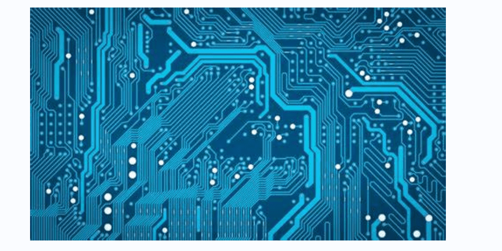
TogglePrinted Circuit Boards (PCBs) are the backbone of modern electronic devices. These boards are used in nearly every electronic device, from smartphones to computers, and are essential to the functioning of these devices. PCBs are used to connect electronic components and provide a platform for them to communicate with each other.
PCB electrical engineering involves the design, development, and manufacture of these boards. PCB engineers use specialized software to design the layout of the board, including the placement of components and the routing of electrical connections. They must also consider factors such as signal integrity, power distribution, and thermal management.
PCB electrical engineering is a complex and challenging field that requires a deep understanding of electronic components and circuit design. With the increasing demand for smaller, faster, and more powerful electronic devices, the role of PCB engineers has become increasingly important. The design and manufacture of PCBs is a critical step in the development of electronic devices, and the success of these devices depends on the quality and reliability of the PCBs used.

PCB Design
PCB design is a crucial aspect of electrical engineering. It involves creating a physical layout of a printed circuit board (PCB) that connects various electronic components. The design process includes schematic capture, layout design, and routing.
Schematic Capture
Schematic capture is the process of creating a graphical representation of an electronic circuit. It involves drawing symbols for each component and connecting them with wires to indicate how they are interconnected. This step is essential as it helps to ensure that the circuit functions as intended and that all components are properly connected.
Layout Design
Layout design involves arranging the components on the PCB. The goal is to minimize the size of the board while ensuring that the components are properly spaced and connected. This step requires careful consideration of the size and shape of each component, as well as the location of any connectors or other external interfaces.
Routing
Routing involves creating the physical connections between the components on the PCB. This step is critical as it determines the electrical performance of the circuit. The routing process involves selecting the appropriate trace widths and spacing to ensure that the circuit can handle the required current and voltage levels.
In summary, PCB design is a complex process that requires careful consideration of many factors. By following best practices for schematic capture, layout design, and routing, engineers can create reliable, high-performance PCBs that meet the needs of their applications.
Electrical Engineering Principles

Circuit Analysis
Circuit analysis is a fundamental concept in electrical engineering. It involves understanding the behavior of electrical circuits and their components. In circuit analysis, we use mathematical techniques to analyze the behavior of circuits, such as Kirchhoff’s laws and Ohm’s law. These techniques help us determine the voltage, current, and power in a circuit.
Signal Integrity
Signal integrity is an important aspect of electrical engineering, especially in high-speed digital circuits. It refers to the ability of a signal to retain its integrity as it travels through a circuit. Signal integrity issues can arise due to various factors such as noise, crosstalk, and reflections. To ensure signal integrity, engineers use various techniques such as impedance matching, signal termination, and shielding.
Power Distribution
Power distribution is a crucial aspect of electrical engineering, as it ensures that electrical power is delivered efficiently and safely to devices. Power distribution involves designing and implementing power distribution systems that can handle the power requirements of devices. Engineers use various techniques such as voltage regulation, power factor correction, and load balancing to ensure efficient power distribution.
In summary, electrical engineering principles such as circuit analysis, signal integrity, and power distribution are essential in designing and implementing electrical systems. Understanding these principles helps engineers ensure that electrical systems are efficient, reliable, and safe.
PCB Fabrication
Substrate Material Selection
When it comes to selecting the substrate material for PCB fabrication, there are a few factors to consider. The most common substrate materials are FR-4, CEM-1, and CEM-3. FR-4 is the most popular choice due to its high-temperature tolerance and low cost. CEM-1 and CEM-3 are similar to FR-4, but have a lower glass transition temperature and are more suitable for low-power applications. Other substrate materials, such as ceramic and metal core PCBs, are used for specific applications that require high thermal conductivity or rigidity.
Etching Process
The etching process involves removing unwanted copper from the PCB using a chemical solution. The first step is to apply a layer of photoresist to the substrate, which is then exposed to UV light through a photomask. The exposed areas of the photoresist become hard and protect the copper underneath, while the unexposed areas remain soft and are removed using a developing solution. The PCB is then immersed in an etchant solution, which dissolves the unprotected copper. After the etching process is complete, the photoresist is removed using a stripping solution.
Drilling
Drilling is the process of creating holes in the PCB for component placement and interconnects. The drilling process is typically done using a computer-controlled drilling machine that drills holes of different sizes and shapes. The holes are then plated with a thin layer of copper to create electrical connections between the different layers of the PCB.
Plating
Plating is the process of depositing a thin layer of metal onto the surface of the PCB. This is done to protect the copper from oxidation and to improve the electrical conductivity of the PCB. The most common metals used for plating are tin, nickel, and gold. Tin is the most popular choice due to its low cost and ease of use. Nickel is used for high-temperature applications, while gold is used for high-reliability applications.
In conclusion, PCB fabrication is a complex process that involves several steps, including substrate material selection, etching, drilling, and plating. The choice of substrate material and plating metal depends on the specific application requirements. The etching and drilling processes are critical for creating the necessary interconnects and component placement.
Testing and Debugging

Functional Testing
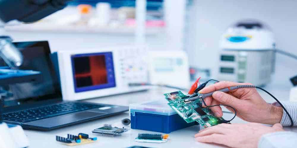
Functional testing is a crucial step in the PCB manufacturing process. It ensures that the board’s components are working as intended and that the circuit is functioning correctly. Functional testing can be done manually or with automated testing equipment.
Manual functional testing involves manually probing the board’s components and measuring their outputs with a multimeter. Automated functional testing, on the other hand, uses testing equipment to automate the testing process. This method is faster and more accurate than manual testing.
Boundary Scan Testing
Boundary scan testing is a non-intrusive testing method that checks the connectivity of a PCB’s components. It is a useful method for testing the board’s interconnectivity and verifying that the components are correctly connected.
Boundary scan testing uses a boundary scan register (BSR) to test the PCB. The BSR is a shift register that can be used to test the connectivity of the board’s components. This method is useful for testing complex boards with many components.
In-Circuit Testing
In-circuit testing is another non-intrusive testing method that checks the functionality of a PCB’s components. It is a useful method for testing the board’s functionality and verifying that the components are working correctly.
In-circuit testing uses a test fixture to test the PCB. The fixture contains probes that make contact with the board’s components and measure their outputs. This method is useful for testing complex boards with many components.
In conclusion, testing and debugging are essential steps in the PCB manufacturing process. Functional testing, boundary scan testing, and in-circuit testing are all useful methods for testing a PCB’s components and verifying that the circuit is functioning correctly.

