The processes to making Printed Circuit Boards (PCBs) are not completed at once. The processes include the making of the earliest designs or schematics, followed by prototypes, fabrication, assembly and final production. However, there is a possibility of making a PCB lamination before all these are over.
Circuit board users are sometimes thrown off as to what the lamination process is all about and what difference it makes. So, we have put together this article to guide you through PCB lamination process.
Before the Lamination Came the Structure
Before a circuit board is laminated, it needs to have a structure. That structure forms a basic of the PCB design, as it aids the connection and support of the different electronic components.
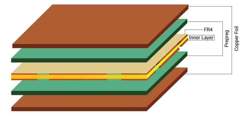
Ideally, these components or parts are made up of different laminates, such as a glass epoxy base material that has a coating of copper on both sides or on one side.
Why is PCB Lamination Important?
There is an urgent need for laminating a Printed Circuit Board (PCB) due to the presence of conductive pathways on the board. These pathways are the medium through which connection is established across the board for the several components.
It is also important to mention that copper sheets are used to etch these conductive pathways. This is the reason why PCB lamination is required to help prevent the copper layer from either conducting a signal or a layer.
The second reason why circuit board lamination is important is due to the stacking presences. Considering that the High Density Interconnect (HDI) process is becoming prevalent in the PCB industry, it is imperative to have a process in place to support the connection of the components.
How Does the PCB Lamination Process Work?
When a circuit board is said to be laminated, it means the processes used to build-up the successive layers of a PCB material. These processes are also used to bind these sequential layers as a way of increasing the waterproofing, strength and protection of a wide range of substances.
How PCB Lamination Prevents Copper-Intrusion
One of the core goals of laminating a PCB, asides from the layer building and binding, is to prevent the copper layer from an inadvertent conduction of a layer or current. For this to happen, the copper must be laminated or attached to the circuit board’s substrate.
Types of PCB Lamination Materials
Several materials are used to laminate a PCB. At the core of the material selection are the following factors or criteria:
- Speed and Weight Considerations: it is important to choose a PCB laminate material that offers a mix of lightweight and higher speeds. That way, the integration and facilitation of the lamination process wouldn’t be difficult.
- Miniaturization: this refers to the process of ensuring the PCB laminate’s reliability by way of using a little space as possible, while working as expected.
- Functionality and Lifecycle: the PCB lamination cycles are also considered. They refer to the duration at which the material’s performance will peak. For the best results, go for the materials that offer a mixture of longer lifecycles and better functionality.
With that being said, here is a list of some of the popular dielectrics or materials you can use when laminating a Printed Circuit Board (PCB):
1. PTFE
Consider using this PCB dielectric if you are working towards laminating circuit boards meant for use with any of the following applications:
- Microwave
- High-frequency and;
- High-power
2. FR-4 Laminate
The Flame Retardant (FR-4) laminate should be used if you are laminating the standard or traditional PCBs. While this is the primary usage, it is also possible to use the FR-4 laminate for other purposes.
For example, if you can go for the versions higher than the regular Tg of 135˚C, you may be able to use the laminate for other applications. For example, FR-4 laminates with a Tg ranging between 150 and 210˚C can be used for laminating the high-density applications.
3. CEM 1-3 Laminates
These laminates are best-used for the circuit boards designated for high-density applications. The Tg ranges from 122˚C and 125˚C.
How to Laminate a PCB

Let us look at some of the steps you can take to make a laminated circuit board.
1. Board Preparation
The PCB needs to be prepared. The process involves washing the panels. This process helps in the removal of the following from the surface:
- Dry film stripping
- Corrosion
- Fingerprints and;
- Anti-foam residues
2. Perform Micro-Etching
This is a minimal etching process. You can use either a black oxide treatment or a standardized brown treatment to do this.
To compare the two, the black oxide treatment is mostly-used due to the reduced risks of delamination. It also helps to improve the adhesion capabilities of the epoxy resin.
The goal of micro-etching a PCB is to minimize or reduce the thickness of the copper.
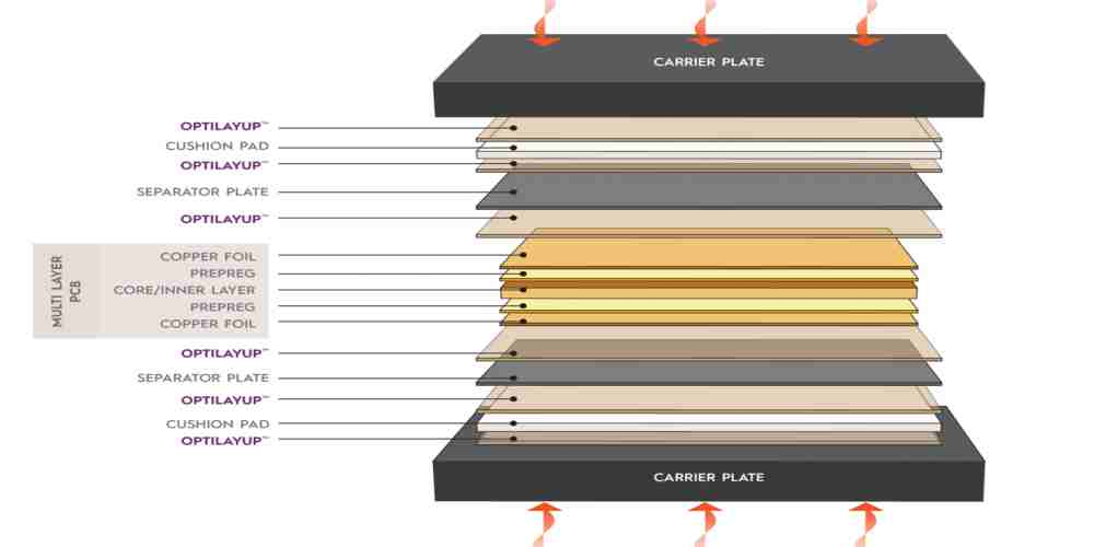
Prepreg and Inner Layers’ Stacking
Now, it is the time to stack or place the inner layers and the prepreg together. The stacking is done on the gluing lamination machine for circuit board.
Once the stacking is done, the inner layers and the prepreg are then glued together.
3. PCB Strengthening
The strengthening of the PCB follows and the process involves the usage of rivets along the unusable board edge. The strengthening process typically entails connecting the inner layers to the prepreg.
The following are also implemented to bolster the PCB’s strength:
- The connection of the prepreg and the inner layers helps to strengthen the stack-up. This also plays an important role towards preventing the stack-up’s movement when it is time to properly laminate the circuit board.
- An application of a stainless-steel patch and prepreg is used to sandwich the copper foil. The completion of this process marks the completion of the PCB’s stack-up.
4. Stack-Up Exposure
The next stage of the PCB lamination process is to expose the built stack-up to extreme temperatures. It is to be noted that the extent of the exposure is to be dictated by the material/dielectric or laminate. To this end, check the datasheet of the materials to get an idea of the exact operating temperature to expose the materials in the stack-up.
5. Layer Unmolding and Preparation
The completion of the stack-up’s exposure signals the start of another process – the unmolding and preparation of the layers.
These inners are first moved onto a cold press where they are to be unmolded before the prepared. This is to be done with registration to be made with an x-ray machine.
6. Panel Deburring
The last stage of the PCB lamination process is the deburring of the panels. Once this is completed, the next process is to round the panels at the corners.
PCB Lamination Types – What Options have You Got?
The processes of laminating the Printed Circuit Board (PCB) can be facilitated via different fronts. Here is a summary of the different types of PCB laminations you can use today:
1. Double-Sided PCBs
This refers to the Printed Circuit Boards (PCBs) with two sides and these two sides can be laminated.
The lamination process requires the use of a photosensitive dry resist under extreme pressure and temperature.
2. Multilayer PCBs
This refers to the multilayer PCB lamination, whereby the circuit boards with several layers are laminated.
Here are some quick points to note about the process:
- The multilayer PCB lamination process is used for both the trace layers and the thin-etched circuit boards.
- Those are then bonded with lamination.
- The lamination process for multilayer PCBs includes placing the layers intense pressure of up to 400 psi. They are also subjected to high-temperature curing of up to 375˚ Fahrenheit.
- The circuit board will be allowed to cure at the higher temperature. Once this is achieved, the pressure will be slowly released. When the material cools, the photosensitive dry resist will be used to laminate the PCB.
3. Teflon (PTFE)
In this type of PCB lamination, the process used mostly is the Chlorotrifluoroethylene (CTFE) thermoplastic film. A pressure of up to 200 psi is usually maintained throughout the duration of the lamination process.
The heating process takes over after that. In this case, the Teflon (PTFE) microwave laminates are heated up to 400˚ Fahrenheit.
Once the curing process is over, the laminates will be cooled.
The following are some of the important pieces of information about the Teflon (PTFE) PCB lamination process:
- It is common to use the Teflon (PTFE) laminates with the Radio Frequency (RF) PCBs. It is also used with the RF circuit boards that have high-speed signal flows.
- The features or characteristics of the PTFE laminates are: reliable dielectric constant, minimal electrical loss and tight depth tolerance.
4. PCB Sequential Lamination
This refers to the lamination process for Printed Circuit Boards (PCBs) possessing two or more subsets. These subsets are the multilayered PCBs that were created in separated processes.
The lamination process includes:
- The creation of the multilayer circuit boards via separate processes.
- Integration of an insulating material between the subsets. This material is usually a dielectric element, which is used to press the subsets together.
- The standard PCB lamination process will then be implemented.
Conclusion
The lamination processes for Printed Circuit Boards (PCBs) may differ, but the end-results are always the same – to bolster the building/stacking of multiple layers and preventing copper’s interruption, in the form of conducting a layer or a signal.
While at it, we at Hillman Curtis pay a special attention to prevent PCB lamination defects, especially the PCB lamination void. This void is created as a result of the weakening of the bond between the copper foil and the prepreg.
We use different processes, including prevention of moisture presence between the layers and making an extensive inner layer drying before laminating the circuit board.
