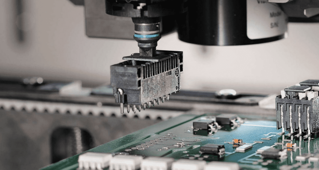
Several steps need following regarding essential steps need to be followed regarding manufacturing. These steps include selecting a board, using the right components, and reflow soldering the board. After this step, the PCB will go to a pick-and-place machine, where it will mount on its pads. Next, the machine feeds the components through component reels that rotate and quickly stick the parts to the board.
The Application of Solder paste
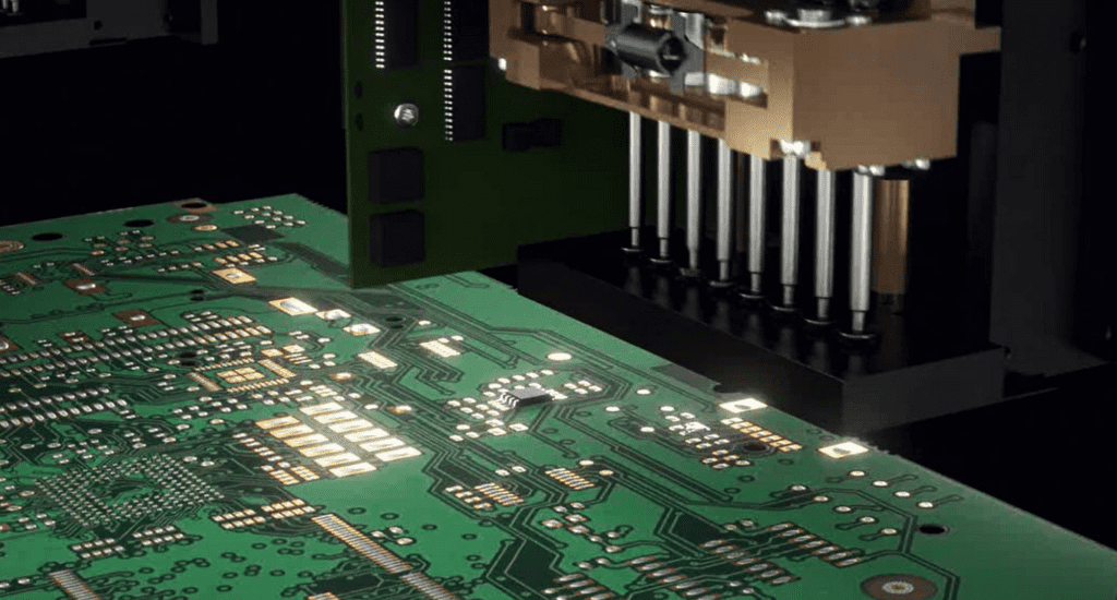
The PCB manufacturing and assembly process involves solder paste application to each component’s contacts. In addition, the components are placed on the PCB using a pick-and-place machine. The pick-and-place machine uses air pressure and a vacuum to pick and place the component on the PCB. Once the component is in place, the solder paste melts and cools to form a proper solder joint.
Printing is the longest in the PCB manufacturing and assembly processes. It typically lasts for fifteen to forty-five seconds. The separation of the stencil is the next longest step. Afterward, we conduct a postprint inspection to verify the deposited solder paste layers are suitable for surface mounting. We usually perform postprint inspections by separate 3D vision systems or unique 2D vision systems on the printer.
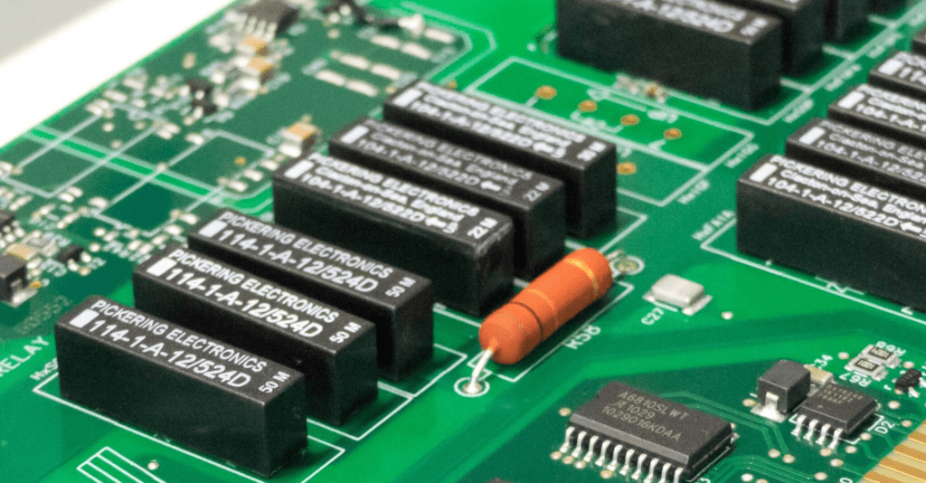
The solder paste consists of metal particles dispersed in a flux. In the past, lead was often helpful in its formulation. However, it is only used in specific industrial settings because it is a hazardous element. Flux is a binding agent that allows electronic components to be on the board’s pads.
Solder paste application is one of the essential PCB manufacturing and assembly stages. Its failure can affect the entire assembly process. Furthermore, we must do solder paste printing to maximize solder paste transfer efficiency. Therefore, it is essential to consider all aspects of the solder paste application process. For instance, improperly applied solder paste will result in a poor-quality PCB.
The squeegee is another essential element in the solder paste application process. Different components have different solder paste requirements, so the squeegee used in soldering differs based on the component type. For example, a fine-pitch component requires much less solder paste volume than a standard component. The thickness of the pads also determines how much solder paste is necessary for soldering.
The importance of the solder mask

In the SMD PCB manufacturing and assembly processes, the solder mask layer covers the PCB pads, which protects them from contamination and oxidation. We usually apply the solder mask layer to the PCB in a blue or peelable form, and we can remove it mechanically or manually. However, the mask is a temporary cover that only covers the PCB and is not a replacement for standard solder resistance.
The process of solder mask manufacture involves various steps. The lowest-cost solder mask application is through the epoxy liquid, silkscreened onto the PCB. The second-cheapest solder mask application uses liquid photo imageable inks, which are vacuum laminated onto the PCB. Both of these processes go through a thermal cure before being applied to the board.
The solder mask is an essential component of the assembly process, but there are some important steps to make sure that the solder mask adheres to the board. First, it is necessary to thoroughly inspect the board to ensure that the solder mask adheres to the surface. When conducting this test, it is essential to use a 1.5 to 10-time magnification.
We treat the solder mask like a layer on the SMD components and describe the process in a Gerber file. We select the mask according to the board’s physical dimensions, component placement, holes, heat sinked power semiconductors, and surface layout. In addition, the final application of the PCB is also an important consideration. Several industries have specific requirements regarding solder masks, so it is essential to understand exactly which is right for your PCB.
To remove the solder mask, you will need a chemical stripping agent. This liquid can erode the solder mask on the copper surface and the substrate. The stripping agent is generally dichloromethane.
The ideal application of Epoxy resin
The process of PCB fabrication involves the use of epoxy resin. The material is ideal for a variety of reasons, including several reasons. The first is to prevent the components from degrading over time. The resin helps maintain the circuit’s structure and electrical properties. It also helps to prevent the oxidation of copper and tin conductors.
Another essential feature of epoxy resin is its ability to insulate components. The material is often a high-quality insulator and can be helpful as a coating on PCBs. Because it is a strong insulator, epoxy resin can make big-sized PCBs. However, the manufacturing process requires special equipment and materials.
PCBs made from epoxy resin are characterized by excellent mechanical and thermal properties. As a result, they can withstand heavier loads than those made from conventional materials. The material also provides insulation and moisture resistance. This feature helps protect the electrical components from dust, heat, and mechanical shocks.
Epoxy resin PCBs are generally more expensive than traditional PCBs, as they use FR-4 substrate material. The substrate is a crucial factor in the manufacturing process. The choice of substrate material will determine the overall performance of the board. As a result, it’s essential to choose the right material for the PCB’s design and components. If you use the wrong substrate, the resulting boards could suffer from fading or even damage.
Understanding the Surface mount components
Surface mount components are electronics components soldered onto SMD components. Compared to their lead-free counterparts, they are smaller and designed to be handled by machines. These devices also feature standard shapes and sizes used throughout the electronics industry. The leading standardization body is JEDEC.
The SMD components assembly process begins with a design phase. After choosing components, the designer must develop SMT patterns. Other software is also available to design printed circuit boards. After completing this step, the PCB assembly data must go to a surface mount manufacturer. In addition to the design, the manufacturer needs to provide the surface finish for the components.
Next, the assembler applies solder paste and places the SMD components on the solder pads. We often package components in trays, tubes, or reels. Pick-and-place machines can also place the components onto the PCB assembly. These machines can also create a bill of materials (BOM) that contains the necessary components for the assembly.
SMD components are also more cost-effective than through-hole components. They are easier to use and require less wire to connect. However, there are a few disadvantages to using surface-mounted components. First, the SMD components are more difficult to rework. If they do break, they require a great deal of skill. Therefore, they are not always viable.
We solder surface mount components to a PCB. First, the solder joints must be robust and durable. They should be able to withstand thermal and mechanical stresses. Second, the components must be safe from moisture. Finally, the assembly process can be automated or manual.
Alternatives to Surface Mount Devices
There are three significant alternatives to Surface Mount Devices. These include Through-hole technology, Standard SMT technology, and Quad Flat Packs. These alternatives are largely unaffected by the size or shape of your integrated circuits. However, each of these alternatives has a particular advantage or disadvantage, and each method has its benefits and drawbacks.
The Basics and Selection of Surface Mount Devices
Surface mount devices are components that are adhered to a printed circuit board surface. They can be either bonded or soldered to the PCB assembly. Depending on the surface mount device type, they can be inexpensive or expensive. A Surface Mount Device can help you quickly and easily make more complex products.
These devices can make your production process more efficient by using suction surfaces to support the SMD components and pick-and-place pads to make the PCB assembly process easier. They also feature a high level of automation, cutting labor costs and increasing production rates. And because they use tape-on-reel packing, you can use them with your existing pick-and-place machines.
Surface mount devices are a popular choice for electronic projects. They add a professional look to your project and help you avoid assembling them by hand. But they’re not the only option. There are also through-hole devices with wire leads sold directly to the PCB assembly.
The use of Through-hole technology in Everyday Life
Through-hole technology is an alternative to surface-mount devices in PCB assembly. It involves drilling holes through the bare PCB and inserting component leads into the holes. This method is less common in today’s consumer electronics but can be very useful in high-end, high-power applications. However, this method is more expensive than surface mount and requires manual and wave soldering. Additionally, it limits the amount of configuration space available on the board.
SMT was first developed in the 1960s and referred to as “Planar Mounting.” This technology works by applying solder paste to the empty pads on the PCB. It eliminates the need for holes in the PCB assembly and is more efficient than through-hole technology.
Through-hole technology is more reliable in many ways. Because we locate the leads on a through-hole component through the board, they are less susceptible to environmental stress than SMT components. As a result, through-hole components are much more durable and suitable for high-reliability products because they are more robust and preferred in military and aerospace applications.
Standard Surface Mount technology in Electronics
Surface Mount technology can produce higher assembly density than traditional through-hole assembly processes. It also has advantages in terms of reliability and reduced electromagnetic interference. Furthermore, it can provide cost savings of 30% to 50%. As a result, this technology is suitable for high-volume manufacturing. To learn more about it, visit our website.
SMT enables manufacturers to mount electronic components on printed circuit boards with less solder. As a result, they can save on space, weight, and process costs. This technology also overcomes many of the limitations of conventional through-hole technology, allowing manufacturers to produce smaller, more expensive, and faster circuit boards.
The main advantages of SMT are small component sizes and better electromagnetic compatibility. They can also be more reliable than plug-in types and can be helpful on smaller circuit boards. In addition, SMT components are about a 10th of the size of the plug-in versions, reducing volume and weight by 60% to 80%. They are also highly reliable and have a low defect rate. Furthermore, they have better high-frequency characteristics, resulting in lower electromagnetic interference.
The Best Quad Flat Packs Considerations
In consumer electronics, the demand for smaller products is increasing. To meet this need, many manufacturers are focusing on miniaturization. We can do this by using smaller, thinner packages. In particular, a quad flat pack no-lead package (QFN) provides superior thermal performance and a smaller board routing area. Moreover, it eliminates the problem of bent leads. Because of these advantages, Texas Instruments has chosen this package type as its miniaturization strategy.
In addition to surface mount devices, another alternative is a heat sink quad flat package. The QFP has four sides, and each side has a connection. This type of package is similar to SMD components except for the pitch and size of leads. The difference between these two types of packages lies in the material used for the leads. In addition, a QFN package has gull-wing leads, which makes it ideal for soldering.
Printed circuit boards have also changed over the years. Now, they can accommodate several components and dense circuitry. However, mounting accuracy is crucial, as a misplaced component can cause short circuits. As a result, it is essential to choose a surface mount device with the right size and shape.
Advantages and Disadvantages of surface mount device and SMT Assembly
SMD components and SMT are two types of assembly techniques. The main difference between the two methods lies in component selection and placement. In SMT, components mount on an electrical board. Additionally, the process lends itself to automation, which increases efficiency and accuracy.
In SMD components, there are no traditional leaded leads. Instead, different components use different package styles, including transistors, diodes, and integrated circuits. Placing these components on the circuit board begins with aligning the PCB stencil. Once aligned, solder paste is applied.
While SMD and SMT are closely related, they are not the same. While both consist of similar materials, SMD components are preferred for many applications because they reduce the overall fabrication cost, space, and time required for a product. The advantages of SMD components are solderable contacts and multicolor encapsulation.
The Size and design of SMD Components
Another difference between SMD components and SMT-based components is the size and design. SMD components can have smaller surface areas and better electromagnetic compatibility. They can also feature many components and achieve high circuit speeds. Furthermore, they use air-cooled conductors. These components are also cheaper to produce and use fewer parts.
Surface Mount Devices (SMDs) are often on a circuit board. This allows them to fit more efficiently and precisely than other electronics components. As a result, using surface mount technology for your electronic projects is a great way to cut costs and complexity.
Surface Mount Technology is a relatively new method of mounting components on circuit boards. It has replaced through-hole technology and is a preferred choice for many electronics makers. The technology uses automation, pick and place machines, and wave or reflow soldering to attach all the components to PCBs. It is also cheaper than through-hole insertion and can be helpful in various applications, such as consumer electronics.
The Performance of SMD Components
SMD components consist of high-performance plastics, which enable them to mount on a PCB automatically. The resulting PCB assembly is highly reliable and smooth. In addition, they don’t require drilling. As a result, the process is fast and cost-effective, allowing more electronics manufacturers to adopt SMT components in their production process.
While both types of devices are helpful in electronics, there are significant differences between SMD and SMT. Surface Mount Devices are often much smaller and cheaper than traditional components and can be more flexible. They also require no wires or leads to connect to them. Moreover, they can fit onto smaller circuit boards.
PCB Assembly method for SMT & SMD components
Another significant difference between SMT and SMD components is the method of assembly. SMT uses a pick-and-place machine to place electronic components on a circuit board. SMD Technology also uses solder paste applied to bare circuit boards. Then, we place the component is placed with solder paste and then reflow soldered. This method is faster, cheaper, and more accurate.
