PCB layout simulation is an essential part of the design process for any electronic circuit. It allows designers to test their designs before committing to a physical prototype, saving both time and money. Simulation software can accurately model the behavior of a circuit, predicting its performance and identifying potential issues before they arise.
One of the key benefits of PCB layout simulation is the ability to visualize the behavior of a circuit. This allows designers to see how signals flow through the circuit, identify potential bottlenecks or areas of high current density, and optimize the layout to improve performance. Simulation software can also predict the effects of environmental factors such as temperature, humidity, and electromagnetic interference, allowing designers to ensure that their circuits will function reliably in real-world conditions.
In addition to improving the performance and reliability of a circuit, PCB layout simulation can also help to reduce development time and costs. By identifying potential issues early in the design process, designers can make changes to the circuit layout or component selection before committing to a physical prototype. This can save both time and money, as well as reducing the risk of costly errors or design flaws.
Basics of PCB Layout Simulation
What is PCB Layout Simulation?
PCB layout simulation is the process of testing and verifying the design of a printed circuit board (PCB) before manufacturing. This process allows designers to identify and correct any potential issues in the design, such as signal integrity problems, power distribution issues, and thermal management problems, before the PCB is manufactured.
PCB layout simulation involves using specialized software tools to create a virtual model of the PCB design and simulate its behavior under different conditions. This allows designers to analyze the performance of the design and make necessary changes to improve its performance and reliability.
Why is PCB Layout Simulation Important?
PCB layout simulation is an essential step in the PCB design process. It helps to ensure that the final product meets the required specifications and performs as expected. By simulating the behavior of the PCB design, designers can identify potential problems early in the design process, which can save time and money in the long run.
PCB layout simulation also helps to reduce the risk of design errors and improve the overall quality of the final product. By identifying potential issues in the design, designers can make changes to improve the performance and reliability of the PCB, ensuring that it meets the needs of the end-user.
In conclusion, PCB layout simulation is a critical step in the PCB design process. It allows designers to test and verify the design of the PCB before manufacturing, identifying and correcting potential issues early in the design process. This helps to ensure that the final product meets the required specifications and performs as expected, reducing the risk of design errors and improving the overall quality of the final product.
Types of PCB Layout Simulation

There are several types of PCB layout simulation that can be used to analyze the behavior of a circuit. Each type of simulation has its own strengths and weaknesses, and the choice of simulation method depends on the specific requirements of the circuit being analyzed.
Transient Analysis
Transient analysis is used to simulate the behavior of a circuit over time. This type of simulation is useful for analyzing circuits that have time-varying signals, such as amplifiers and filters. Transient analysis can be used to determine the response of a circuit to a step input, a pulse input, or any other time-varying input signal.
DC Analysis
DC analysis is used to simulate the behavior of a circuit under steady-state conditions. This type of simulation is useful for analyzing circuits that have constant or slowly varying signals, such as power supplies and voltage regulators. DC analysis can be used to determine the voltage and current levels in a circuit, as well as the power dissipated by each component.
AC Analysis
AC analysis is used to simulate the behavior of a circuit under sinusoidal conditions. This type of simulation is useful for analyzing circuits that have high-frequency signals, such as RF amplifiers and filters. AC analysis can be used to determine the gain and phase response of a circuit, as well as the frequency response of each component.
Monte Carlo Analysis
Monte Carlo analysis is used to simulate the behavior of a circuit under random conditions. This type of simulation is useful for analyzing circuits that have components with wide tolerance ranges, such as resistors and capacitors. Monte Carlo analysis can be used to determine the statistical distribution of circuit parameters, such as voltage and current levels, and can help identify potential failure modes.
In summary, the choice of simulation method depends on the specific requirements of the circuit being analyzed. Transient analysis is used for time-varying signals, DC analysis is used for steady-state conditions, AC analysis is used for high-frequency signals, and Monte Carlo analysis is used for components with wide tolerance ranges.
PCB Layout Simulation Tools

When designing a printed circuit board (PCB), it is important to simulate the layout to ensure proper functionality and performance. There are several simulation tools available, each with their own unique features and benefits.
SPICE
SPICE (Simulation Program with Integrated Circuit Emphasis) is a widely used simulation tool for electronic circuits. It can simulate both analog and digital circuits and is known for its accuracy. SPICE can be used to simulate a PCB layout and analyze its performance. It is available in both free and paid versions.
TINA
TINA (Texas Instruments Network Analyzer) is a simulation tool designed specifically for analog circuits. It can simulate PCB layouts and provide accurate results. TINA also includes a library of components and models, making it easy to design and simulate circuits. It is available in both free and paid versions.
LTSpice
LTSpice is a simulation tool developed by Linear Technology. It can simulate both analog and digital circuits and is known for its speed and accuracy. LTSpice can be used to simulate PCB layouts and analyze their performance. It is available for free.
PSPICE
PSPICE is a simulation tool developed by Cadence Design Systems. It is widely used in the electronics industry and can simulate both analog and digital circuits. PSPICE can be used to simulate PCB layouts and analyze their performance. It also includes a library of components and models. PSPICE is available in both free and paid versions.
In conclusion, there are several simulation tools available for PCB layout simulation, each with their own unique features and benefits. It is important to choose the right tool for the job to ensure accurate results.
PCB Layout Simulation Process
Schematic Capture
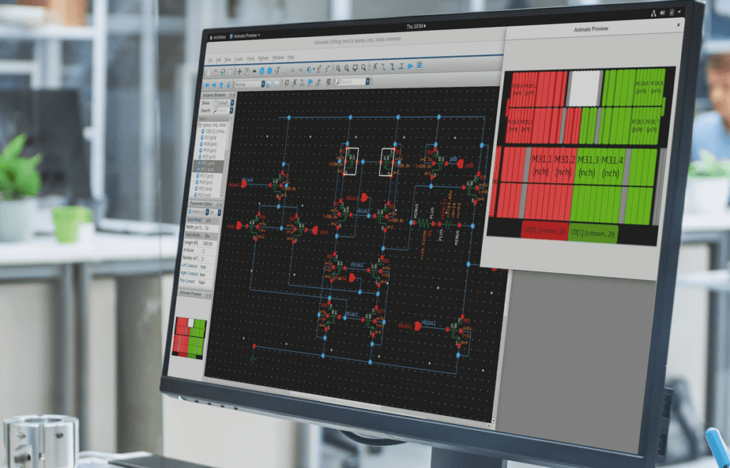
The first step in the PCB layout simulation process is to create a schematic diagram of the circuit. This is typically done using a schematic capture tool, which allows the designer to create a graphical representation of the circuit using symbols and lines to represent components and connections. The schematic capture tool also allows the designer to add important information such as component values and part numbers.
Netlist Generation
Once the schematic diagram is complete, the designer must generate a netlist. This is a list of all the components in the circuit and their connections, which is used by the simulation software to create a virtual representation of the circuit. The netlist can be generated automatically by the schematic capture tool or manually by the designer.
Simulation Setup
After the netlist is generated, the designer must set up the simulation parameters. This includes selecting the simulation type (such as transient or frequency domain), defining the simulation time or frequency range, and specifying any simulation options or settings.
Simulation Run
With the simulation parameters set up, the designer can run the simulation. This process can take anywhere from a few seconds to several hours, depending on the complexity of the circuit and the simulation settings. During the simulation run, the software calculates the behavior of the circuit over time or frequency.
Results Analysis
Once the simulation is complete, the designer can analyze the results. This includes reviewing waveforms, calculating key performance metrics, and identifying any issues or areas for improvement. The designer can then make changes to the circuit and repeat the simulation process until the desired performance is achieved.
Overall, the PCB layout simulation process is an essential step in the design of complex electronic circuits. By simulating the behavior of the circuit before it is physically built, designers can save time and money while ensuring that the circuit meets its performance requirements.
PCB Layout Simulation Best Practices

Keep it Simple
When it comes to PCB layout simulation, it’s best to keep things as simple as possible. Start with a simple design and gradually add complexity as you become more comfortable with the simulation process. This will help you avoid overwhelming yourself and ensure that you can properly analyze your results.
Start Small
Start with a small section of your PCB layout and simulate that section first. This will help you identify any issues early on and make any necessary adjustments before you move on to the entire layout. It’s also a good idea to simulate each section individually before combining them to ensure that everything is working properly.
Use Realistic Models
When simulating your PCB layout, it’s important to use realistic models for all components. This will help ensure that your simulation accurately reflects the behavior of the actual circuit. Use manufacturer datasheets to obtain the necessary information for each component and make sure to include parasitic components such as capacitance and inductance.
Verify Your Results
After simulating your PCB layout, it’s important to verify your results. This can be done by comparing your simulation results with actual measurements taken from the physical circuit. If there are any discrepancies, go back and re-evaluate your simulation setup and make any necessary adjustments.
Document Your Work
Finally, it’s important to document your work throughout the simulation process. This includes keeping track of all simulation settings and results, as well as any changes made to the layout. This documentation will be useful for future reference and can help you avoid making the same mistakes in future designs.
By following these best practices, you can ensure that your PCB layout simulation is accurate and reliable, helping you to create successful designs.
