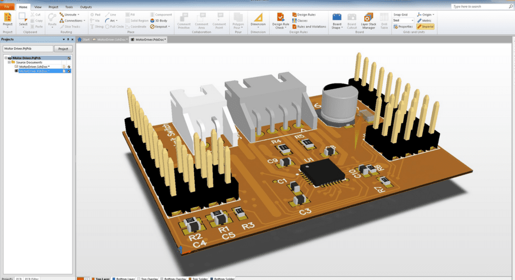
Altium Designer is a popular software tool used for designing printed circuit boards (PCBs). It offers a comprehensive set of features that make it easy for designers to create and optimize high-quality PCB layouts. The software provides an intuitive user interface that allows designers to easily navigate through the design process, from schematic capture to PCB layout and routing.
One of the key benefits of using Altium Designer is its ability to automate many of the tedious and time-consuming tasks associated with PCB layout. For example, the software can automatically route traces, place components, and generate design rule checks (DRCs) to ensure that the layout meets industry standards and best practices. This automation can save designers a significant amount of time and effort, allowing them to focus on more complex design tasks.
Another advantage of using Altium Designer is its extensive library of components and templates. The software comes with a vast library of pre-built components and templates, which can be easily customized to meet the specific needs of a project. This library can help designers save time and reduce errors, as they can quickly find and use components that have already been tested and verified. Overall, Altium Designer is a powerful and versatile tool that can help designers create high-quality PCB layouts efficiently and effectively.
Basics of PCB Layout
Understanding Altium Designer
Altium Designer is a powerful software tool used to create printed circuit board (PCB) layouts. It is a comprehensive software package that includes schematic capture, PCB layout, and design verification tools. Altium Designer is widely used in the electronics industry for designing high-quality PCBs.
Creating a New PCB Layout
To create a new PCB layout in Altium Designer, you need to start by creating a new project. Once you have created a new project, you can start adding schematics and PCB layouts to it. To create a new PCB layout, you can select the “New PCB Layout” option from the “File” menu.
Importing Schematic into PCB Layout
To import a schematic into a new PCB layout, you can use the “Import Changes from Schematic” option in the “Design” menu. This will import the schematic into the PCB layout and automatically place the components on the board. You can then adjust the placement of the components as needed.
Placing Components on PCB Layout
To place components on a PCB layout, you can use the “Place” option in the “Tools” menu. This will open a component library where you can select the components you want to place on the board. You can then drag and drop the components onto the board and adjust their placement as needed.
In summary, Altium Designer is a powerful software tool used to create high-quality PCB layouts. To create a new PCB layout, you need to start by creating a new project and importing a schematic. You can then place components on the board and adjust their placement as needed.
Routing and Tracing

Routing Traces
Routing traces is a crucial aspect of PCB layout design. Altium Designer provides an intuitive and easy-to-use routing feature that allows designers to route traces quickly and efficiently. The routing feature provides various routing modes, including interactive, manual, and auto-routing. Interactive routing provides the most control over the routing process, allowing designers to adjust the routing path in real-time. The manual routing mode offers complete control over the routing process, allowing designers to place and route traces manually. The auto-routing mode is ideal for simple designs, and it automatically routes traces based on the design rules.
Adding Vias
Adding vias is essential for connecting traces on different layers of the PCB. Altium Designer provides an easy way to add vias to the design. Designers can add vias by selecting the via tool and placing the via on the PCB. The via properties can be adjusted to match the design requirements, including the size, shape, and drill size. Vias can also be added to the design by converting a pad to a via.
Creating Copper Pour
Copper pour is a technique used to create a continuous copper plane on the PCB. The copper plane can be used for ground planes, power planes, or signal planes. Altium Designer provides an easy way to create copper pours. Designers can create copper pours by selecting the copper pour tool and drawing a polygon on the PCB. The copper pour properties can be adjusted to match the design requirements, including the net, clearance, and fill style.
In conclusion, Altium Designer provides an easy-to-use routing feature that allows designers to route traces quickly and efficiently. Adding vias is essential for connecting traces on different layers of the PCB, and creating copper pour is a technique used to create a continuous copper plane on the PCB. These features make Altium Designer an excellent tool for PCB layout design.
Design Rule Checking
Setting up Design Rules
Design Rule Checking (DRC) is a crucial step in PCB layout design. It helps to ensure that the design meets the required specifications and standards. Altium Designer provides a powerful DRC engine that allows designers to set up various design rules for their projects.
To set up design rules in Altium Designer, go to the “Design” menu and select “Rules”. This will open the “PCB Rules and Constraints Editor” window. From here, you can create and modify rules for different design aspects such as clearance, routing, and impedance.
Running Design Rule Check
After setting up the design rules, the next step is to run the DRC to check for any violations. To do this, go to the “Tools” menu and select “Design Rule Check”. This will open the “Design Rule Check” window, where you can select the rule set to use and run the check.
During the DRC process, the software will highlight any violations found in the design. The violations can be viewed in the “Messages” panel, where details of the error and its location can be found.
Fixing Design Rule Errors
When DRC errors are found, they need to be fixed before proceeding with the design. The “Messages” panel provides information on the error and its location, making it easier to locate and fix the problem.
To fix DRC errors, you can use various methods such as adjusting the routing, changing the component placement, or modifying the design rules. Once the errors are fixed, the DRC can be run again to ensure that all violations have been resolved.
In conclusion, Design Rule Checking is an essential step in PCB layout design. Altium Designer provides a powerful DRC engine that allows designers to set up and check various design rules. By following the steps outlined above, designers can ensure that their designs meet the required specifications and standards.
Finalizing PCB Layout
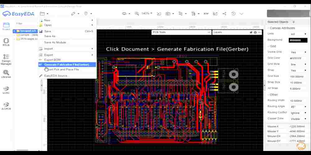
Generating Gerber Files
Once you have completed your PCB layout in Altium Designer, you need to generate Gerber files. Gerber files are the industry standard for PCB manufacturing. They contain all the information needed to fabricate your PCB, including the copper layers, solder mask, and silkscreen.
To generate Gerber files in Altium Designer, go to File > Fabrication Outputs > Gerber Files. In the Gerber Setup dialog box, select the layers you want to include in the Gerber files and set the output directory. Then click OK to generate the Gerber files.
Creating Assembly Drawing
An assembly drawing is a detailed drawing that shows the components, their placement, and the connections between them. It is used by the manufacturer to assemble the PCB.
To create an assembly drawing in Altium Designer, go to File > Fabrication Outputs > Assembly Drawings. In the Assembly Drawing Setup dialog box, select the layers you want to include in the assembly drawing and set the output directory. Then click OK to generate the assembly drawing.
Exporting PCB Layout
Once you have generated the Gerber files and assembly drawing, you need to export the PCB layout. The PCB layout is exported as a single file that contains all the information needed to recreate the PCB in Altium Designer.
To export the PCB layout in Altium Designer, go to File > Fabrication Outputs > ODB++. In the ODB++ Setup dialog box, select the layers you want to include in the PCB layout and set the output directory. Then click OK to export the PCB layout.
In conclusion, finalizing your PCB layout in Altium Designer involves generating Gerber files, creating an assembly drawing, and exporting the PCB layout. These steps are critical for ensuring that your PCB is manufactured correctly.
