PCB transformer design is an essential process in the development of electronic devices. The design of a transformer is critical in ensuring that the electronic device operates efficiently and effectively. A transformer is a device that transfers electrical energy from one circuit to another through electromagnetic induction.
PCB transformers are widely used in electronic devices such as power supplies, audio amplifiers, and other electronic circuits. The design of a PCB transformer involves selecting the right core material, wire size, and number of turns to ensure that the transformer meets the required specifications. The design process also involves considering factors such as the operating frequency, voltage, and current. A well-designed PCB transformer can improve the efficiency and performance of an electronic device.
PCB Transformer Design Fundamentals
PCB transformers are important components in electronic circuits that are used to transfer electrical energy from one circuit to another through electromagnetic induction. They are widely used in power supplies, audio amplifiers, and other electronic devices.
The design of a PCB transformer involves several key factors, including the number of turns, the wire gauge, the core material, and the winding configuration. These factors need to be carefully considered to ensure that the transformer operates efficiently and reliably.
One of the most important considerations in PCB transformer design is the number of turns. The number of turns determines the voltage ratio between the primary and secondary windings, and it is critical to achieving the desired output voltage. The wire gauge is also important, as it affects the current-carrying capacity of the transformer and the resistance of the windings.
The core material is another critical factor in PCB transformer design. The core material affects the magnetic properties of the transformer and determines its efficiency and performance. Common core materials include ferrite, powdered iron, and laminated iron.
Finally, the winding configuration is also important in PCB transformer design. The winding configuration affects the coupling between the primary and secondary windings and determines the transformer’s impedance and frequency response.
In summary, PCB transformer design involves several key factors that need to be carefully considered to ensure that the transformer operates efficiently and reliably. These factors include the number of turns, the wire gauge, the core material, and the winding configuration. By paying attention to these factors, designers can create high-performance transformers that meet the requirements of their electronic circuits.
Design Considerations
When designing a PCB transformer, there are several critical design considerations that must be taken into account. These considerations can be broadly divided into two categories: electrical parameters and physical parameters.
Electrical Parameters
The electrical parameters of a PCB transformer are critical to its performance. These parameters include:
- Turns ratio: The turns ratio determines the voltage transformation ratio of the transformer and is calculated as the ratio of the number of turns on the secondary winding to the number of turns on the primary winding.
- Inductance: The inductance of the transformer determines its ability to store energy in its magnetic field and is a function of the number of turns, the core material, and the physical dimensions of the transformer.
- Leakage inductance: Leakage inductance is the inductance associated with the magnetic field that does not link the primary and secondary windings and is an important consideration in high-frequency applications.
- Resistance: The resistance of the transformer windings must be minimized to reduce power losses and improve efficiency.
- Frequency response: The frequency response of the transformer determines its ability to transmit signals across a range of frequencies and is a function of the inductance and capacitance of the transformer.
Physical Parameters
The physical parameters of a PCB transformer are equally important and include:
- Core material: The core material determines the magnetic properties of the transformer and is typically made of materials such as ferrite, powdered iron, or laminated steel.
- Winding geometry: The winding geometry of the transformer must be carefully designed to minimize leakage inductance and maximize coupling between the primary and secondary windings.
- Wire size: The wire size of the transformer windings must be chosen to minimize resistance and power losses while still fitting within the physical constraints of the transformer.
- Physical size: The physical size of the transformer must be optimized to fit within the available space on the PCB while still meeting the electrical requirements of the application.
By carefully considering these electrical and physical parameters, designers can create high-performance PCB transformers that meet the specific needs of their applications.
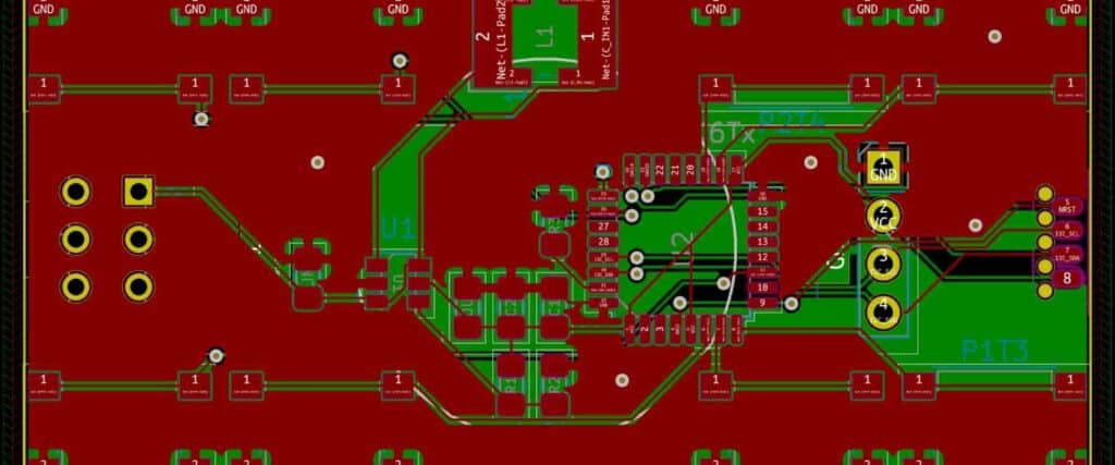
PCB Layout Guidelines

When designing a PCB transformer, it is important to consider the layout of the printed circuit board. Here are some guidelines to follow:
-
Keep the transformer close to the driver circuit: This reduces the length of the traces between the driver and the transformer, which helps minimize parasitic inductance and capacitance.
-
Keep the traces short: Short traces reduce the parasitic inductance and capacitance, which can negatively affect the performance of the transformer.
-
Keep the traces wide: Wide traces have lower resistance, which reduces the power dissipation and improves the efficiency of the transformer.
-
Use a ground plane: A ground plane can help reduce noise and provide a low impedance return path for the current.
-
Avoid crossing traces: Crossing traces can create unwanted coupling and increase the parasitic capacitance.
-
Use a star ground: A star ground can help reduce noise and provide a single point of reference for the ground.
-
Use a guard trace: A guard trace can help reduce the parasitic capacitance between the primary and secondary windings.
-
Avoid sharp corners: Sharp corners can create unwanted coupling and increase the parasitic capacitance.
By following these guidelines, you can improve the performance and efficiency of your PCB transformer design.
Simulation and Testing
Simulation and testing are essential steps in the PCB transformer design process. Simulation software can help to predict the transformer’s performance, allowing designers to optimize their design before building a physical prototype.
One popular simulation software is LTSpice, which is free and easy to use. LTSpice allows designers to model a transformer’s behavior under different conditions, such as varying load currents and frequencies. This information can help designers to choose the best transformer topology and windings for their application.
After simulating the transformer design, it’s important to test the physical prototype to ensure that it meets the desired performance specifications. A common test is to measure the transformer’s efficiency, which is the ratio of output power to input power. Other tests may include measuring the transformer’s voltage and current levels under different loads and frequencies.
Designers can use an oscilloscope and a function generator to perform these tests. An oscilloscope can measure the transformer’s voltage and current waveforms, while a function generator can provide a known input signal to the transformer.
In conclusion, simulation and testing are crucial steps in PCB transformer design. Simulation software such as LTSpice can help designers to optimize their design, while physical testing can ensure that the transformer meets the desired performance specifications.
Advanced Techniques
When designing PCB transformers, there are several advanced techniques that can be used to improve the transformer’s performance. These techniques are particularly useful when designing transformers for high-frequency applications.
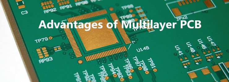
Multi-Layer PCBs
Using multi-layer PCBs can help reduce the size of the transformer and improve its performance. By using multiple layers, the designer can create a more complex winding pattern, which can help reduce leakage inductance and increase the transformer’s coupling coefficient. Additionally, multi-layer PCBs can provide better thermal management, which can help improve the transformer’s efficiency.
Planar Transformers
Planar transformers are another advanced technique that can be used to improve transformer performance. Planar transformers are constructed using flat, layered windings, which can help reduce leakage inductance and increase the transformer’s coupling coefficient. Additionally, planar transformers can be designed to have a low profile, which can be useful in applications where space is limited.
Magnetic Shielding
Magnetic shielding is an advanced technique that can be used to reduce the amount of electromagnetic interference (EMI) generated by the transformer. Magnetic shielding involves placing a shield around the transformer to block the magnetic field. This can be particularly useful in applications where the transformer is in close proximity to other sensitive electronic components.
High-Frequency Materials
Using high-frequency materials, such as ferrite or powdered iron, can help improve transformer performance at high frequencies. These materials have a higher permeability than traditional materials, which can help reduce the size of the transformer and improve its efficiency. Additionally, high-frequency materials can help reduce EMI and improve the transformer’s thermal management.
Overall, these advanced techniques can help improve the performance and efficiency of PCB transformers, particularly in high-frequency applications. By using these techniques, designers can create transformers that are smaller, more efficient, and generate less EMI.
