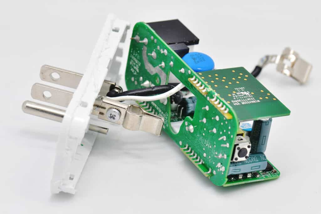
If your next device can run on a solar element, battery power, or it plugs in the wall, it is important that you design circuitry so as to regulate the power that leads into your device. Furthermore, PCB power supply design has the ability to encompass not just the actual power supply. They can also encompass systems that range from our personal computers to the different home appliances requiring a power supply in converting the walls’ AC power to the DC power with extremely low noise.
Furthermore, the PCB power supply design isn’t just about converting AC to DC power and vice versa. There’s a need to consider power as well as signal integrity issues, and the thermal management problems arising with respect to high power electronics. The truth is that power and signal integrity are related because of the manner in which the ICs operate and function. Also, there are power supplies which can deliver great radiated EMI, which will affect the remaining parts of the circuit board.
There’s no power supply as well as the system linked to it can be immune from power integrity and signal integrity problems. However, with the implementation of some procedures for simple design, it prevents a redesign. Working with these practices has to do with everything relating to proper arrangement of the component to the bypassing/decoupling, and the stackup design.
Main Functions of PCB Power
The main functions of printed circuit board PCB power include the following.
- Converts AC to DC voltage using either full wave or half rectification
- Disturbs the appropriate DC voltage to all the components present in any electronic appliance
- Steps voltages down or up making use of the transformer to the AC line voltage you desire
- Regulates the output power supply to the applied load
- Filters the pulsating DC voltage into a steady and pure DC voltage to be useful in different equipment
- Providing some voltage division form so as to meet the requirements of the equipment
What Are The Important Additional Circuit Modules for the PCB Power Supply?
Rectifier Blocks
They are useful in converting the AC (alternating current) to DC (direct current) by allowing the device’s current flow to go in just one direction.
Power Factor Control Circuit Blocks
The power factor control blocks help in compensating the lagging current using capacitors to the creation and supply of the leading current. Also, this capacitance must be very close to unity.
Input Filter Circuits
The major purpose of this is preventing an electromagnetic interference which is created through the switching source from gaining access to the power rail and power line as well as causing problem for the device. Also, they prevent any high-frequency voltage that is present on power lines (transmission lines) from passing through the output of the power supply
Control and Feedback Circuit Blocks
These circuit blocks help in controlling a device’s output making use of its value as feedback signal. You can then reference this feedback signal to a different signal therefore creating an error signal. The controller then filters the signal in generating the system’s control input.
Output Regulator Circuits
These are useful in maintaining a steady voltage level output without considering the quantity of current that is drawn away from your power supply. Furthermore, it monitors the current the load draws then increases or decreases the voltage therefore keeping the level of voltage constant.
Output Filter Circuit Blocks
These circuit blocks help in smoothing out the ripples in the rectified DC. This helps in generating the direct and even current. This type of current is great even for the very sensitive circuits.
Overcurrent and Overvoltage Protection Blocks
The fuses and circuit breakers are useful in preventing overvoltage while the low-power small comparison circuit deals with the under voltage.
What are the Options for the PCB Power Supply Design?
The first ever step for power supply has to do with choosing the power supply type that you want to use with your device. Power supplies that are unregulated are a down and dirty alternative for the conversion of AC power from any wall outlet to the DC voltage. Also, these supplies’ output will have in them a form of ripple waveform serving as its output isn’t smoothed with any regulator. Also, the modern applications make use of a regulated power supply, whereby the ripple is reduced.
Two major options exist for the regulation of DC output from the power supplies. This makes use of the switching regulator or linear regulator that can be referred to as the switch-mode power supply.
Also, these forms of power supplies help in passing the DC output from the wave rectifier to the regulation circuit. This helps in smoothing that ripple waveform, which is usually superimposed onto your desired DC output.
More Options
Furthermore, these regulators are useful in regulating the DC power source directly such as the battery. The linear regulators also feature an extremely low noise, however they could be bulky as a result of the heatsinks used or some other cooling measures that are necessary for thermal management. Also, a huge heat dissipation occurring in the power supplies is what leads to their low efficiency.
Furthermore, in contrast, the power supply (switched mode) offers more efficiency when placed over a wide current range. This allows the power supplies to have a smaller form factor. Moreover, the power supplies make use of a PWM circuit in smoothening and regulating its output voltage. This needs the utilization of the active switching component (usually a MOSFET).
What this means is that the system usually radiates a strong EMI. Also, the output contains spikes as a result of the switching noise. The switching noise could show as the ringing signal present on an output (for example, the conducted EMI). Also, this noise will have to be filtered off from that output.
What are the Main Considerations When Designing PCB Power?
You must design an effective PCB power in a way that ensures it offers clean power as well as minimal noise. Below are some of the considerations for the design.
Noise
To reduce the possibility of an EMI that creates noise for the entire board, there is a need to make use of the most compact of packages. Furthermore, the tightest, most optimized component placement, as well as shorter routing plays a huge role in noise reduction.
Current
The PCB Power usually involves very high current levels. What this means is that, you must use adequate trace widths and copper weight to handle it.
Heat
The power supply gets hot all the time. This design must be in such a way that the PCB power supply dissipates so much heat.
Layer Stackup
The ground planes or power plane has to fall between the power supply’s components and routing and its inner layer having delicate signals.
Useful in multilayered PCB configuration
This plane serves as a protection for the delicate traces of the signal from the routing present on outer layers as well as from the noisy power components.
Trace Routing
You complement the direct short traces placement by routing. The traces for your current have to be very wide. You should use 45 degrees and rounded corners in substituting the right angles. Furthermore, avoid using vias, because they add inductance as the power traces.
Components Placement
Components must be kept very close to each other. This helps in reducing the trace’s length, and close to those appliances receiving the load. Also, the parts must be placed in a specific way so that the path’s power is straight and small through them.
Challenges Experienced During the Lead-Free Soldering of PCB Power Assembly Using Large Components
Usually, components that have large volume and mass present a form of preheating problem. Furthermore, they take time in heating up due to their large mass. Some other components are usually heat starved till these large components heat up adequately.
This shadow effect creates some results during improper soldering. This is because the small components don’t heat up enough. In addition, the heavy copper tracks need more heat in reaching optimum temperature before the soldering as a result of its high mass.
If you don’t achieve the required preheat temperature, the pads solder wont melt improperly, and the components won’t stick onto them.
Reasons Why You Should Place the PCB Power Components Closer Together When Assembling
It is important to keep these parts close to helps in reducing the trace’s length as well as close to devices receiving the load. This makes sure that the power’s path passes through them directly and is also short.
Also, you place the input capacitor near the integrated circuit which is present on one layer. This inductor must also share the same layer with the IC, and must stay near it.
You must position the output capacitor proximately close to the inductor. This helps in reducing the routing. Once you are through placing the main board’s components, the PCB power supply’s residual parts are placed very close
Ways in Which the Heavy Copper Track Affect the Assembly Process of the PCB Power
As a result of the large mass, this copper track usually needs extra heat to be able to reach the temperatures you desire before soldering
The solder present on the heavy copper tracks’ pads won’t melt properly when the tracks don’t reach the optimum preheat temperatures. What this means is these components don’t adhere to solder
Furthermore, there is a need to adjust the thermal profiles for these assemblies passing through the reflow machine so as to allow them to heat up sufficiently before you reach the soldering zone.
Also, this might need fixing of the thermocouples on some specific points present on the PCB power. This holds most especially on larger components and heavy copper traces. This helps in assessing the temperature change nature undergone during the reflow machine path.
What are the Best Practices for Your PCB Power Supply Design
For the low power applications, the switching regulators and linear regulators come as ICs (integrated circuits). These integrated circuits are great or different mobile devices as well as other which may plug in the wall outlet but needs low power consumption.
Even with your device’s power consumption, you have to take some important PCB design considerations into account. This is to make sure that there is signal integrity and power integrity.
With respect to the regulator type that is used in the power supply, you should consider adding some circuits to the board. Also, there are some simple choices for the layout which helps in surpassing the radiated and conducted EMI.
For the extreme case, like the power supply of high current or with the switching regulator, you might have to add some shielding to the circuit board to make sure that there is signal integrity in the circuits nearby.
Thermal & Power Integrity Used in PCB Power Supply Design
The PCB power supply design is something more than power conversion. Also, making sure that there is power integrity in the power supply output helps in solving signal integrity issues. Also, thermal management is important for power supplies to serve as components that can dissipate heat all through the process of conversion.
How to Choose a Regulator During the PCB Power Supply Design
Any output from the switching and linear regulators has to do with some noise although the effects and source of the noise on downstream circuits varies. The linear regulator features less noise, however, it also dissipates extra heat and it is less efficient.
The switching regulator on the other hand helps in replacing the input’s ripple for the output’s switching noise. Moreover, the output voltage can be controlled easily from the switching regulator. This is possible through the adjustment of the PWM signal duty cycle that ensures the switching action. This switching regulator helps in dissipating lesser heat due to its extremely high efficiency.
Options of Thermal Management for the Large Regulated Power Supplies
With these power supplies of high current, there’s a great chance that you will be building the regulator circuit you required from some discrete components. This is because the system size will be extremely large in fitting in the standard package for integrated circuit.
For these cases, there will be a need to work with some thermal management options for the integrated circuit in the PCB of the power supply. Furthermore, for the conversion of power from wall outlets to the DC, there is a simple solution, which is mounting a fan on that enclosure and then powering it with the use of an input AC signal. With the DC to DC power supplies, there’s a need for PWM signals in running the fan for cooling your components.
Also, the layer stack plays a significant role in thermal management. Using the multilayer board to design the power supply PCB will ensure thermal management. This is because the copper plane layers aid in distributing the heat evenly all through the circuit board.
Making use of thermal vias below the components dissipating a large quantity of heat could assist in transporting heat away from the components quickly. Furthermore, the goal here is the prevention of hot spots forming on the board by allowing quick dissipation of heat from the critical components
Decoupling and Bypassing For Power Integrity
Immediately you send power downstream to the components, different active components can lead to ringing and ground bounce in the power bus when the ICs switch
This could cause bit rate errors whenever large ICs switch simultaneously at the same time it affects the power the components receives as well as the potential difference present between the OFF and ON states in the digital signals
Furthermore, integrated circuits running at a lower voltage supply are usually very prone to encountering these issues. This is because of the smaller voltage difference present between the OFF and ON states in the digital signals
You can solve all these issues by designing the decoupling network, as well as selecting bypass capacitors in-between the power pins and ground pins on an integrated circuit. This goal in the placement of the bypass capacitors is compensating the changes present in that ground potential whenever many ICs switch simultaneously. Power pins
Similarly, the designing of the decoupling network is done to transient oscillations. For example, ringing occurs in the power bus whenever the integrated circuits on the bus switches. A very important tool for designing the power delivery network as well as decoupling network is using circuit analysis tools in designing the RLC network forming these circuits.
With the appropriate choices for the component, you will be able to damp the transient oscillations critically in the power delivery network as well as compensate for the ground bounce.
Conducted EMI Suppression
The noise output that comes from the regulator or the unregulated power supply has the ability to affect the conducted EMI and downstream components. Hash noise coming from the power bus could affect the downstream components’ output level.
Furthermore, large switching noise and ripple voltages present in the switching regulator could create the problems, most especially whenever the power supply offers high current. Also, for cases like this, the conducted EMI has to be filtered off the output of power supply. Since, generally, one prefers the DC output, the filtration is useful in taking out the high frequency components from the output of power supply. Here, simulations for the filters are now important. This is because it helps in choosing those components that you need for the building of your filter.
Shielding with the Switching Regulators
The switching regulators help in emitting EMI, which will be able to affect the signal integrity present in the downstream circuits. This occurs most especially in the analog components. The switching regulators of low levels might not create many issues unless you place them near the sensitive components.
Moreover, the power supplies having high output current could lead to an involuntary switching in the digital circuits nearby or the noise spikes present in the analog circuits that look like a transient response in nearby circuits.
Furthermore, the band stop filtering present at the natural frequency of the circuit could be effective at getting rid of the present spikes. However, this isn’t practical when working with many components on the printed circuit board.
Rather, taking advantage of the shielding offered by the power and ground planes in the layer stack and then arranging the sensitive components at a farther distance from its switching regulator is easier. Also, there may be a need to add some shielding on the sensitive components when they are close to the switching regulator. This is because they will block the radiated EMI. Ground planes
RayMing PCB & Assembly PCB Power Supply Design

The layout rules are necessary to ensure power and signal integrity in the power supply as well as the whole circuit board, there is a need to have the right layout, analysis, and design tools, which will adapt to the application. Furthermore, the PCB power supply design tools and analysis tools should take the data from the schematic directly, and then help you to determine the most appropriate layout choices for the system.
The complete printed circuit board PCB design as well as analysis tools suite are adaptable to all applications. These include the high speed design. Also, you will be opportune to have access to the full electronics design as well as analysis solution whenever you are working with the industry-standard design tools of Rayming PCB & Assembly.
If you really wish to learn more concerning Rayming PCB & Assembly’s perfect solution for you, then speak to our professional team. We will be glad to be of help.
Conclusion
PCB power is very important in the electronics industry and PCB manufacturing processes today. PCB power supply design has the ability to encompass not just the actual power supply. They can also encompass systems that range from our personal computers to the different home appliances.
