Power amplifier PCB layout is a critical aspect of designing a high-quality audio amplifier. The PCB layout affects the performance of the amplifier and can make the difference between a good amplifier and a great one. The layout of the PCB can affect the noise, distortion, and stability of the amplifier.
The power amplifier PCB layout is important because it determines the placement of components and their interconnections. A good layout can minimize the noise and distortion generated by the amplifier, while a poor layout can increase noise and distortion. The layout can also affect the stability of the amplifier, which is important for preventing oscillations and ensuring reliable operation. Therefore, it is essential to pay close attention to the PCB layout when designing a power amplifier.
Design Considerations
PCB Size and Shape
The size and shape of the PCB play an important role in the overall performance of the power amplifier. The PCB should be designed in such a way that it can accommodate all the necessary components without compromising the overall performance. The size of the PCB should be chosen according to the size of the enclosure in which it will be placed. The shape of the PCB should be such that it can fit snugly inside the enclosure without any overlapping or bending of components.
Ground Planes
The ground plane is an essential component of the power amplifier PCB layout. It helps in reducing the noise and interference in the circuit. The ground plane should be designed in such a way that it covers the entire PCB. The ground plane should be connected to the power supply ground through a single point. This will help in reducing the ground loop noise. The ground plane should also be kept away from the high-frequency components to avoid any interference.
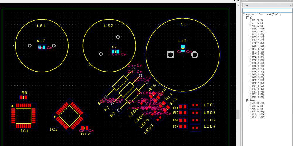
Component Placement
The placement of the components on the PCB is crucial for the overall performance of the power amplifier. The components should be placed in such a way that the signal paths are kept as short as possible. The power supply components should be placed near the power input connector to reduce the noise and interference. The input and output components should be placed at a distance from each other to avoid any crosstalk. The high-frequency components should be placed away from the low-frequency components to avoid any interference.
In conclusion, the size and shape of the PCB, the ground planes, and the component placement are crucial design considerations for a power amplifier PCB layout. By following these design considerations, one can ensure the optimal performance of the power amplifier.
Trace Routing

When designing a power amplifier PCB layout, trace routing is a critical step that can significantly impact the performance of the amplifier. Proper trace routing ensures that signals are delivered to the components with minimal noise and distortion. In this section, we will discuss the key considerations for trace routing.
Trace Width and Spacing
The width and spacing of the traces on the PCB play a critical role in determining the performance of the amplifier. The width of the traces determines the amount of current that can flow through the trace without causing excessive heating. The spacing between the traces determines the amount of crosstalk between the traces.
To ensure proper trace width and spacing, the designer should consult the manufacturer’s datasheet for the components used in the amplifier. The datasheet will provide guidance on the recommended trace width and spacing based on the current and frequency of the signal.
Signal Integrity
Signal integrity is critical in power amplifier design. The integrity of the signal can be compromised by noise and distortion caused by improper trace routing. To ensure proper signal integrity, the designer should follow the best practices for trace routing, such as minimizing the length of the traces, avoiding sharp corners, and using ground planes.
Power and Ground Traces
The power and ground traces are critical in power amplifier design. The power traces should be designed to handle the maximum current that the amplifier will draw. The ground traces should be designed to minimize the impedance of the ground path.
To ensure proper power and ground traces, the designer should follow the manufacturer’s guidelines for the components used in the amplifier. The designer should also use ground planes to minimize the impedance of the ground path.
In summary, trace routing is a critical step in power amplifier PCB layout. The designer should pay close attention to trace width and spacing, signal integrity, and power and ground traces to ensure optimal performance.
Noise Reduction Techniques
When designing a power amplifier PCB layout, it is essential to consider noise reduction techniques to ensure that the output signal is clean and free from unwanted noise. Here are some effective noise reduction techniques that can be used:
Filtering Capacitors
Filtering capacitors are used to filter out noise and unwanted signals from the power supply. They are typically placed at the input and output of the power amplifier circuit. The capacitors should have a high enough capacitance value to filter out the noise frequencies effectively. The value of the capacitor should be selected based on the frequency range of the noise that needs to be filtered.
Star Grounding
Star grounding is a technique used to reduce the ground noise in the amplifier circuit. In this technique, all the ground connections in the circuit are connected to a single point, which is then connected to the ground plane. This technique ensures that all the ground connections in the circuit have the same potential, which reduces the ground noise.
Shielding
Shielding is another technique used to reduce noise in the amplifier circuit. It involves enclosing the amplifier circuit in a shielded box or using a shielded cable. The shielded box or cable provides a barrier that prevents the external noise from entering the circuit.
In summary, filtering capacitors, star grounding, and shielding are effective noise reduction techniques that can be used in power amplifier PCB layout design. By implementing these techniques, the output signal of the amplifier circuit can be kept clean and free from unwanted noise.
Thermal Management

Heat Sinks
Heat sinks are an essential component of power amplifier PCB layout. They help dissipate heat generated by the amplifier circuit, ensuring that the components do not overheat and malfunction. Heat sinks are typically made from materials such as aluminum or copper, which have high thermal conductivity. The heat sink is mounted on top of the amplifier transistor, and a thermal interface material is used to improve heat transfer between the transistor and the heat sink.
When selecting a heat sink, it is important to consider the thermal resistance of the heat sink and the maximum operating temperature of the amplifier circuit. A heat sink with a low thermal resistance will provide better heat dissipation, allowing the circuit to operate at a lower temperature. Additionally, the heat sink should be designed to provide adequate airflow to prevent heat buildup.
Thermal Pads
Thermal pads are another important component of power amplifier PCB layout. They are used to improve heat transfer between the amplifier transistor and the heat sink. Thermal pads are typically made from materials such as silicone or graphite, which have high thermal conductivity.
When selecting a thermal pad, it is important to consider the thickness and thermal conductivity of the pad. A thicker pad will provide better heat transfer, but may also increase thermal resistance. Additionally, the thermal pad should be designed to fit the specific dimensions of the amplifier transistor and heat sink.
Overall, proper thermal management is critical for the reliable operation of power amplifier circuits. By selecting appropriate heat sinks and thermal pads, designers can ensure that their circuits operate at a safe temperature, preventing premature failure and improving overall performance.
Testing and Validation
When designing a power amplifier PCB layout, it is essential to test and validate the circuit to ensure that it meets the requirements of the application. The testing and validation process involves functional testing and performance testing.
Functional Testing
Functional testing is the process of verifying that the power amplifier circuit performs the intended functions. The following tests should be performed during functional testing:
- Power Supply Voltage Test: Verify that the power supply voltage is within the specified range.
- Input Signal Test: Verify that the input signal is within the specified range.
- Output Signal Test: Verify that the output signal is within the specified range.
- Protection Circuit Test: Verify that the protection circuit is working correctly.
Performance Testing
Performance testing is the process of verifying that the power amplifier circuit meets the performance requirements. The following tests should be performed during performance testing:
- Gain Test: Verify that the gain of the power amplifier is within the specified range.
- Frequency Response Test: Verify that the frequency response of the power amplifier is within the specified range.
- Distortion Test: Verify that the distortion of the power amplifier is within the specified range.
- Noise Test: Verify that the noise of the power amplifier is within the specified range.
In conclusion, testing and validation are critical steps in designing a power amplifier PCB layout. By performing functional testing and performance testing, you can ensure that the power amplifier circuit meets the requirements of the application.
