TDA2030 is a popular monolithic integrated circuit that can be used as an audio amplifier. Its low distortion, high output power, and low cost make it a popular choice among hobbyists and professionals alike. However, to get the best performance out of the TDA2030, it is important to pay attention to the PCB layout.
The TDA2030 amplifier PCB layout can have a significant impact on the performance of the amplifier. A good layout can minimize noise, reduce distortion, and improve overall sound quality. On the other hand, a poor layout can lead to unwanted noise, distortion, and other issues that can degrade the performance of the amplifier. Therefore, it is important to understand the key principles of PCB layout and how they apply to the TDA2030 amplifier.
TDA2030 Amplifier PCB Layout Design
Schematic Diagram
Before designing a PCB layout for the TDA2030 amplifier, it is important to have a clear and accurate schematic diagram. The schematic diagram should include all the necessary components, their values, and their connections. A well-designed schematic diagram will make the PCB layout process easier and more efficient.
PCB Design Considerations
When designing a PCB layout for the TDA2030 amplifier, there are several important considerations to keep in mind. First, the PCB should be designed to minimize noise and interference. This can be achieved by using a ground plane and keeping signal traces as short as possible. Second, the PCB should be designed to provide adequate heat dissipation for the TDA2030 chip. Finally, the PCB should be designed to be easy to assemble and maintain.
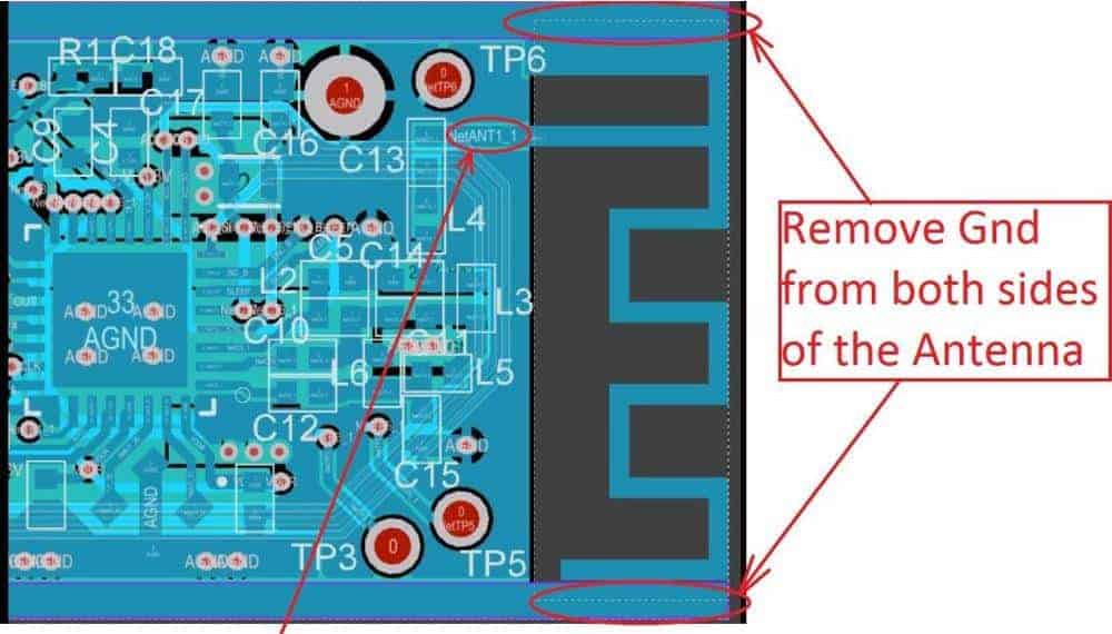
Grounding and Power Supply Layout
The grounding and power supply layout are critical components of the TDA2030 amplifier PCB design. The grounding scheme should be designed to minimize ground loops and noise. The power supply layout should be designed to provide clean, stable power to the TDA2030 chip. A well-designed grounding and power supply layout will ensure that the TDA2030 amplifier operates at its best.
Component Placement and Traces
The placement of components and traces on the PCB is critical to the performance of the TDA2030 amplifier. Components should be placed to minimize noise and interference. Traces should be kept as short as possible to minimize signal loss and interference. A well-placed and routed PCB will ensure that the TDA2030 amplifier operates at its best.
Heat Dissipation and Cooling
The TDA2030 chip generates a significant amount of heat, so it is important to design the PCB to dissipate heat effectively. This can be achieved by using a heatsink, adding thermal vias, and providing adequate ventilation. A well-designed heat dissipation and cooling system will ensure that the TDA2030 amplifier operates at its best.
In conclusion, designing a PCB layout for the TDA2030 amplifier requires careful consideration of several factors, including the schematic diagram, PCB design considerations, grounding and power supply layout, component placement and traces, and heat dissipation and cooling. By paying attention to these factors, it is possible to design a PCB that will ensure the TDA2030 amplifier operates at its best.
Testing and Troubleshooting
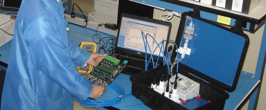
Testing the Amplifier PCB
Once you have assembled the TDA2030 amplifier PCB, it is important to test it to ensure that it is working properly. To test the amplifier, you will need a multimeter, an audio source, and a speaker. Follow the steps below to test the amplifier:
- Connect the audio source to the input of the amplifier PCB.
- Connect the speaker to the output of the amplifier PCB.
- Turn on the amplifier and adjust the volume to a low level.
- Use the multimeter to measure the voltage at the output of the amplifier PCB. The voltage should be around half of the power supply voltage.
- Increase the volume gradually and check that the voltage at the output of the amplifier PCB increases proportionally.
- If the voltage at the output of the amplifier PCB does not increase proportionally, there may be a problem with the amplifier PCB.
Common Issues and Solutions
Here are some common issues that you may encounter when testing the TDA2030 amplifier PCB and their solutions:
| Issue | Solution |
|---|---|
| No sound from the speaker | Check the audio source, the speaker, and the connections between them. |
| Distorted sound from the speaker | Check the volume level and adjust it to a lower level. Check the connections between the PCB and the speaker. |
| Low volume from the speaker | Check the volume level of the audio source and the amplifier. Check the connections between the PCB and the speaker. |
| Overheating of the amplifier PCB | Check the power supply voltage and make sure it is within the specified range. Check the heat sink and make sure it is properly attached to the TDA2030 chip. |
By following the steps above and troubleshooting any issues that arise, you can ensure that your TDA2030 amplifier PCB is working properly and producing high-quality audio.
