Table of Contents
TogglePower electronics is a field of study that focuses on the design and development of electronic circuits that can handle high power levels. These circuits are used in a wide range of applications, from renewable energy systems to electric vehicles. One of the key components of power electronics is the printed circuit board (PCB).
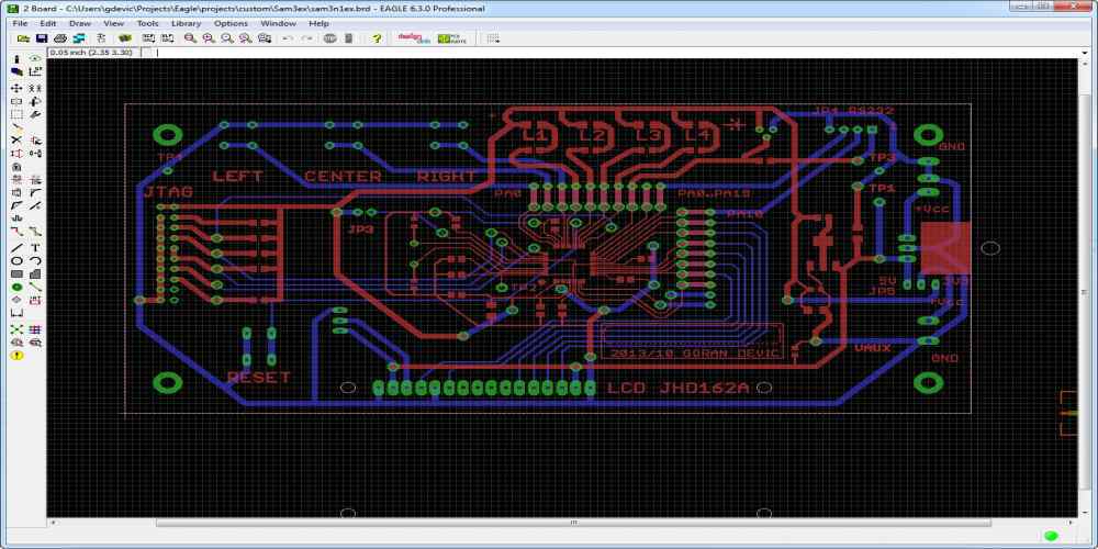
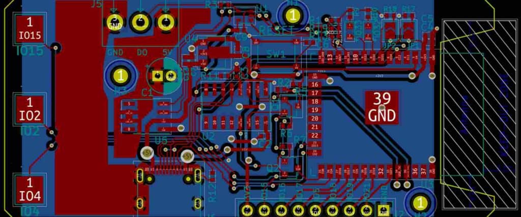
PCBs are used to connect the various components of a power electronics circuit, providing both mechanical support and electrical connections. Designing a PCB for power electronics requires a deep understanding of the unique challenges and requirements of high-power circuits. These circuits generate significant heat, which can cause components to fail if not properly managed. Additionally, high-power circuits require careful attention to component placement and routing to ensure proper operation and reliability.

Basics of Power Electronics PCB Design
Understanding Power Electronics PCBs
Power electronics PCBs are specialized printed circuit boards that are designed to handle high power levels. They are used in applications such as motor drives, power supplies, and inverters. These PCBs are designed to handle high current and high voltage levels, and they require careful consideration during the design process.
Power electronics PCBs are different from standard PCBs in several ways. They often have thicker copper traces, larger vias, and specialized components such as power MOSFETs and IGBTs. These components require special attention during the layout process, as their placement and routing can have a significant impact on the performance of the circuit.
Design Considerations for Power Electronics PCBs
When designing power electronics PCBs, there are several important considerations to keep in mind. These include:
-
Thermal Management: Power electronics circuits generate a lot of heat, and it is essential to manage this heat to prevent damage to the components. Thermal management techniques such as heatsinks, thermal vias, and copper pours can be used to dissipate heat from the circuit.
-
High Current Traces: Power electronics PCBs often have high current traces that require careful routing and placement. These traces should be kept as short and wide as possible to minimize resistance and inductance.
-
Component Placement: The placement of components on a power electronics PCB can have a significant impact on the performance of the circuit. Components such as power MOSFETs and IGBTs should be placed close to the heat sink and other thermal management components.
-
EMI/EMC: Power electronics circuits can generate electromagnetic interference (EMI) and electromagnetic compatibility (EMC) issues. Proper grounding, shielding, and filtering techniques should be used to minimize these issues.
In conclusion, designing power electronics PCBs requires careful consideration of several important factors, including thermal management, high current traces, component placement, and EMI/EMC. By following these design considerations, designers can create robust and reliable power electronics circuits that meet the requirements of their applications.
Components Selection for Power Electronics PCB Design

Choosing the Right Components
When designing a power electronics PCB, it is crucial to choose the right components to ensure optimal performance and reliability. The following are some of the key factors to consider when selecting components:
- Voltage and current ratings: Components must be able to handle the voltage and current levels in the circuit without failing or degrading.
- Temperature range: Components must be able to operate within the specified temperature range without overheating or malfunctioning.
- Size and package: Components must fit within the available space on the PCB and be compatible with the chosen assembly process.
- Cost: Components must be cost-effective and within the budget of the project.
Sizing Components for Power Electronics PCBs
The size of components in a power electronics circuit is critical for proper operation and reliability. The following are some guidelines for sizing components:
- Capacitors: Capacitors should be sized to handle the maximum voltage and current in the circuit. They should also have a low equivalent series resistance (ESR) to minimize losses and improve performance.
- Inductors: Inductors should be sized to handle the maximum current in the circuit without saturating. They should also have a low resistance to minimize losses.
- Diodes: Diodes should be sized to handle the maximum current and voltage in the circuit. They should also have a low forward voltage drop to minimize losses.
- Transistors: Transistors should be sized to handle the maximum current and voltage in the circuit. They should also have a low on-resistance to minimize losses.
In summary, selecting the right components and sizing them correctly is critical for the performance and reliability of power electronics PCBs. By considering the factors mentioned above, designers can ensure that their circuits operate optimally and within specifications.
Layout and Routing for Power Electronics PCB Design
PCB Layout Guidelines for Power Electronics
When designing a PCB for power electronics, there are several layout guidelines that should be followed. These guidelines include:
- Keeping the high current paths as short and wide as possible to reduce the resistance and inductance of the traces.
- Placing the components that generate the most heat, such as power transistors and diodes, near the edge of the board to facilitate heat dissipation.
- Separating the low voltage and high voltage sections of the board to prevent noise and interference.
- Using a ground plane to provide a low impedance return path for the high current traces and to reduce the loop area of the signals.
- Placing decoupling capacitors as close as possible to the power pins of the components to reduce the noise and ripple.
Routing Techniques for Power Electronics PCBs
Routing the traces on a power electronics PCB requires careful consideration to ensure proper functionality and reliability. Some routing techniques that can be used include:
- Using wide traces for high current paths to reduce the resistance and inductance.
- Avoiding sharp angles in the traces to reduce the parasitic capacitance and inductance.
- Routing the traces in a way that minimizes the loop area to reduce the electromagnetic interference (EMI).
- Using a star grounding topology to minimize the ground loop and reduce the noise.
- Using thermal vias to connect the copper planes to the thermal pads of the components to facilitate heat dissipation.
By following these layout and routing guidelines, a power electronics PCB can be designed to operate efficiently and reliably.
Thermal Management for Power Electronics PCB Design

Thermal Considerations for Power Electronics PCBs
Thermal management is a critical aspect of power electronics PCB design. Power electronics circuits generate a significant amount of heat, which can cause damage to components, reduce their lifespan, and even lead to circuit failure. Therefore, it is essential to consider thermal management from the early stages of PCB design.
One of the first steps in thermal management for power electronics PCBs is to select the right materials. The thermal conductivity of the PCB material is crucial in dissipating heat generated by power electronics circuits. Materials with high thermal conductivity, such as aluminum or copper, are ideal for power electronics PCBs. In contrast, materials with low thermal conductivity, such as FR-4, should be avoided.
Another critical consideration is the placement of components on the PCB. Components that generate the most heat, such as power transistors or diodes, should be placed far apart from each other to prevent heat buildup. Additionally, components should be placed in areas with good airflow to facilitate heat dissipation.
Heat Sink Design for Power Electronics PCBs
Heat sinks are commonly used in power electronics PCBs to dissipate heat generated by components. A heat sink is a passive component that transfers heat from the component to the surrounding air. The effectiveness of a heat sink depends on its design, material, and size.
The design of a heat sink should be optimized for the specific component it is cooling. For example, a heat sink for a power transistor should have a large surface area to transfer heat efficiently. The material of the heat sink should have high thermal conductivity, such as aluminum or copper.
The size of the heat sink is also crucial. A larger heat sink can dissipate more heat than a smaller one. However, the size of the heat sink should be balanced with other design considerations, such as available space on the PCB.
In conclusion, thermal management is a critical aspect of power electronics PCB design. Proper thermal management can improve the reliability and lifespan of power electronics circuits. By selecting the right materials and optimizing the design of heat sinks, designers can ensure that their power electronics PCBs operate at optimal temperatures.
Testing and Validation for Power Electronics PCB Design

Validation Techniques for Power Electronics PCBs
Validation of power electronics PCB design is a crucial step in ensuring that the design meets the required performance specifications. The following are some of the common validation techniques for power electronics PCBs:
-
Functional Testing: This involves testing the PCB under normal operating conditions to ensure that it meets the required performance specifications. The testing should cover all the critical functions of the PCB.
-
Environmental Testing: This involves subjecting the PCB to various environmental conditions such as temperature, humidity, and vibration to ensure that it can operate reliably under different conditions.
-
EMI/EMC Testing: This involves testing the PCB for electromagnetic interference (EMI) and electromagnetic compatibility (EMC) to ensure that it meets the required standards.
-
Reliability Testing: This involves subjecting the PCB to accelerated life testing to ensure that it can operate reliably over its expected lifespan.
Testing Considerations for Power Electronics PCBs
Testing of power electronics PCBs is a critical step in ensuring that the design meets the required performance specifications. The following are some of the testing considerations for power electronics PCBs:
-
Power Supply: Ensure that the power supply used for testing the PCB is capable of supplying the required voltage and current levels.
-
Test Equipment: Use appropriate test equipment such as oscilloscopes, signal generators, and power analyzers to accurately measure the performance of the PCB.
-
Test Setup: Ensure that the test setup is properly configured to accurately simulate the operating conditions of the PCB.
-
Test Procedures: Develop test procedures that cover all the critical functions of the PCB and ensure that the procedures are repeatable and reliable.
In conclusion, testing and validation of power electronics PCB design is critical to ensure that the design meets the required performance specifications. By following the validation techniques and testing considerations outlined above, designers can ensure that their designs are reliable, meet the required standards, and can operate under different environmental conditions.

