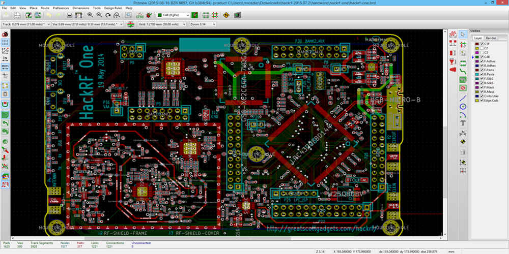
Power PCB layout is a critical aspect of electronic design that can have a significant impact on the performance of a product. A well-designed power PCB layout can improve efficiency, reduce noise, and increase reliability. On the other hand, a poorly designed layout can result in power losses, signal integrity issues, and even damage to components.
To ensure a successful power PCB layout, designers must consider various factors such as component placement, trace routing, and ground planes. They must also be familiar with the different types of power supplies and how to properly route power and ground connections. With the increasing demand for high-speed and high-power electronics, the importance of proper PCB layout cannot be overstated.
Basics of Power PCB Layout
Understanding Power Requirements
When designing a power PCB layout, it is important to understand the power requirements of the circuit. This includes the voltage and current requirements, as well as the power dissipation. The voltage and current requirements will determine the size of the traces and the components needed, while the power dissipation will determine the thermal considerations.
Designing for High Currents
When designing for high currents, it is important to use wider traces and larger components. This will help to reduce the resistance and minimize the voltage drop across the traces. It is also important to consider the placement of components, as this can affect the current flow and create hot spots. Using multiple vias can help to distribute the current and reduce the risk of hot spots.
Thermal Considerations
Thermal considerations are important in power PCB layout, as high power dissipation can lead to overheating and component failure. To minimize the risk of overheating, it is important to use components with a low thermal resistance and to design the PCB with adequate heat dissipation. This can be achieved by using thermal vias, heat sinks, and copper pours.
In summary, understanding the power requirements, designing for high currents, and considering thermal factors are essential when designing a power PCB layout. By following these basic principles, you can ensure that your circuit operates efficiently and reliably.
Components Placement
When designing a power PCB layout, component placement is a crucial aspect that can greatly impact the performance and reliability of the circuit. In this section, we’ll discuss the placement of some key components.
Decoupling Capacitors
Decoupling capacitors are used to filter out noise and stabilize voltage fluctuations. They should be placed as close as possible to the power pins of the IC they are decoupling. Placing them too far away can result in increased inductance, which can reduce their effectiveness.
Inductors and Transformers
Inductors and transformers are used to filter out noise and provide isolation in power circuits. They should be placed as close as possible to the components they are serving. Keep in mind that inductors can generate magnetic fields that can interfere with nearby components, so it’s important to place them away from sensitive components.
Power Connectors
Power connectors are used to connect the power source to the circuit. They should be placed in a location that is easily accessible and allows for easy connection and disconnection. It’s also important to ensure that the connector is rated for the appropriate voltage and current levels.
In summary, proper component placement is critical for a well-designed power PCB layout. By following best practices for decoupling capacitors, inductors and transformers, and power connectors, you can ensure optimal performance and reliability of your circuit.
| Component Type | Placement Recommendations |
|---|---|
| Decoupling Capacitors | Close to power pins of IC |
| Inductors and Transformers | Close to components they are serving, away from sensitive components |
| Power Connectors | Easily accessible, rated for appropriate voltage and current levels |
Routing Techniques

Power Plane Design
The power plane design is an essential aspect of power PCB layout. It provides a stable and low impedance power distribution network. The power plane should be designed to provide the required power to all components on the board. The power plane should be placed adjacent to the ground plane to minimize the inductance and provide a low impedance path for the return current.
Traces Width and Spacing
The width and spacing of the traces are critical for the performance of the power PCB. The width of the trace should be determined by the maximum current that it will carry. The spacing between the traces should be wide enough to prevent any arcing or short circuits. A good rule of thumb is to use a trace width of at least 0.006 inches for every 1 amp of current.
Grounding Techniques
Grounding is an essential aspect of power PCB layout. The ground plane should be designed to provide a low impedance path for the return current. The ground plane should be placed adjacent to the power plane to minimize the inductance and provide a low impedance path for the return current.
One of the most common grounding techniques is the star grounding technique. In this technique, all the ground connections are made at a single point, which is then connected to the ground plane. This technique minimizes the ground loop and provides a low impedance path for the return current.
Another grounding technique is the split-plane grounding technique. In this technique, the ground plane is split into two parts, one for the analog circuit and the other for the digital circuit. This technique minimizes the interference between the analog and digital circuits.
In summary, power PCB layout requires careful consideration of the power plane design, trace width and spacing, and grounding techniques. Proper implementation of these techniques can result in a stable and low impedance power distribution network.
Signal Integrity
EMI/EMC Considerations
When designing a power PCB layout, it is important to consider the potential for electromagnetic interference (EMI) and electromagnetic compatibility (EMC) issues. These can arise due to the high-frequency signals present on the board, as well as external sources of electromagnetic noise. To mitigate these issues, several design considerations should be taken into account:
- Grounding: Proper grounding techniques should be used to minimize the potential for ground loops and other sources of noise.
- Shielding: Shielding can be used to protect sensitive components from external sources of electromagnetic noise.
- Filtering: Filtering components such as capacitors and inductors can be used to suppress high-frequency noise.
Signal Integrity Analysis
Signal integrity is critical in power PCB layouts, as high-frequency signals can degrade and cause issues such as signal distortion and timing errors. To ensure signal integrity, several analysis techniques can be used:
- Transmission line analysis: Transmission line analysis can be used to model the behavior of high-frequency signals on the PCB and ensure that they are properly terminated to prevent reflections.
- Eye diagram analysis: Eye diagram analysis can be used to visualize the quality of high-speed signals and identify potential issues such as signal distortion and timing errors.
- Crosstalk analysis: Crosstalk analysis can be used to identify potential sources of interference between signals on the PCB.
Crosstalk and Noise
Crosstalk and noise can be major issues in power PCB layouts, as high-frequency signals can couple between adjacent traces and cause interference. To mitigate these issues, several design considerations should be taken into account:
- Trace spacing: Adequate spacing between traces can reduce the potential for crosstalk and interference.
- Ground planes: Ground planes can be used to provide a shield between traces and reduce the potential for interference.
- Filtering: As mentioned previously, filtering components can be used to suppress high-frequency noise and reduce the potential for interference.
Testing and Validation

Power Integrity Testing
Power integrity testing is an essential step in the design process of any PCB layout. It helps ensure that the power delivery network (PDN) is correctly designed and that the voltage and current requirements of the components are met. Power integrity testing involves measuring the voltage and current waveforms at various points on the board to identify any potential issues with the PDN.
One of the most common techniques used in power integrity testing is voltage drop analysis. This involves measuring the voltage drop across the power planes and vias to ensure that the voltage is within the acceptable range. Another technique is current profiling, which involves measuring the current flow through the board to ensure that it is within the limits specified by the components.
Signal Integrity Testing
Signal integrity testing is another critical aspect of PCB layout design. It involves measuring the quality of the signals transmitted through the board to ensure that they meet the requirements of the components. Signal integrity testing is essential for high-speed designs, where even small signal distortions can cause significant issues.
One of the most common techniques used in signal integrity testing is time-domain reflectometry (TDR). This involves sending a signal through the board and measuring the reflections to identify any impedance mismatches or other issues. Another technique is eye diagram analysis, which involves measuring the quality of the signal by looking at the shape of the eye diagram.
EMI/EMC Testing
EMI/EMC testing is essential for ensuring that the PCB layout does not interfere with other electronic devices. It involves measuring the electromagnetic emissions and susceptibility of the board to identify any potential issues. EMI/EMC testing is particularly important for designs that will be used in sensitive environments, such as medical equipment or aerospace systems.
One of the most common techniques used in EMI/EMC testing is radiated emissions testing. This involves measuring the electromagnetic emissions from the board using an antenna to ensure that they are within the acceptable limits. Another technique is conducted emissions testing, which involves measuring the emissions through the power and signal lines.
Overall, testing and validation are critical steps in the PCB layout design process. By performing power integrity testing, signal integrity testing, and EMI/EMC testing, designers can ensure that their designs meet the requirements of the components and are safe to use in a variety of environments.
Advanced Power PCB Layout
When designing a power PCB, it is important to consider the various factors that can affect its performance. This section will cover some advanced design considerations that can help optimize the layout of your power PCB.
High Voltage Design Considerations
When dealing with high voltage circuits, it is important to take into account the potential for arcing and breakdown. This can be mitigated by increasing the clearance and creepage distances between traces and components. Additionally, the use of specialized high voltage capacitors and resistors can help prevent voltage spikes and other issues.
RF and Microwave Design Considerations
RF and microwave circuits require careful attention to layout and component placement in order to minimize signal loss and interference. Proper grounding and shielding are critical, as is the use of high-quality components and materials. It is also important to avoid sharp corners and sudden changes in trace width, as these can cause reflections and other issues.
Mixed Signal Design Considerations
When combining analog and digital signals on a single PCB, it is important to separate the two domains as much as possible. This can be accomplished through the use of separate power and ground planes, as well as careful placement of components and traces. Additionally, the use of decoupling capacitors can help reduce noise and interference.
In conclusion, designing an advanced power PCB requires careful attention to a variety of factors, including high voltage considerations, RF and microwave design considerations, and mixed signal design considerations. By following best practices and utilizing high-quality components and materials, you can ensure the optimal performance of your power PCB.
