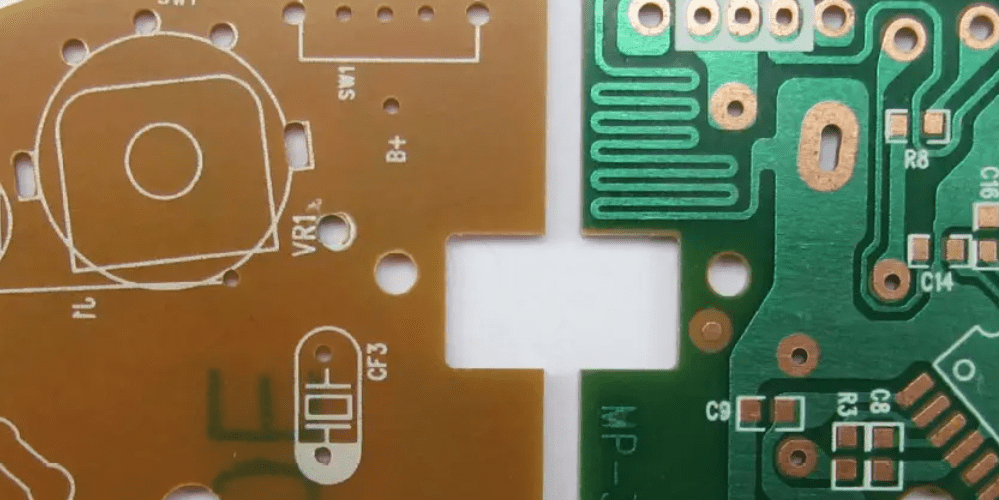
Single PCB fabrication has to do with the creation of bare boards which serves as a foundation for the printed circuit board assembly.
Also, you need to choose the contractor for your single PCB fabrication carefully, because small errors can bring damage to the whole board. This will make the final product become useless. The communication formed between the manufacturers and design team is important, most especially as the manufacturing has been transferred and moved overseas.
For the purpose of this article, we will be taking a look into everything you have to understand regarding the process of single PCB fabrication. These include the pre-process, full single pcb fabrication, as well as some considerations you have to make whenever you are making a choice regarding companies offering a single pcb fabrication company
What is the Process of Single PCB fabrication?
Laser Direct Imaging as well as Etch/Develop/Strip Process
Before you start work on your multilayer PCB, the use of laser direct imaging is necessary for areas which will become the metal ground, pads, and traces of the printed circuit board.
- You apply the dry film onto the copper laminate
- The laser direct imaging helps in exposing some of the circuit board’s part to light in shape of the pattern of the PCB
- The board’s unexposed parts will then develop off, thereby leaving the rest film as the etch barrier
- Also, the film left acts as a form of etch barrier, which will be taken out of the copper that has been exposed. This will form your copper circuitry
Immediately you are done with this, the automated optical inspection helps in inspecting the layers for any defect before laminating them together. When there are errors like opens or shorts, you can still correct them at this particular stage or level.
Lamination and Oxide
After etching all the layers, you will apply a chemical treatment referred to as oxide to the printed circuit board’s inner layers. This helps in improving the bond strength
Then, you laminate the copper foil and prepreg’s alternating layers altogether with the use of a hydraulic press and heat.
In addition, prepreg is known as a form of fiberglass material that contains epoxy resin, which melts as a result of pressure and heat of lamination, therefore bonding these layers in a “PCB sandwich”.
Also, there is a need for careful attention. This is to make sure that you maintain the alignment of the circuitry found in-between each of the layers.
Drilling
To ensure that multilayer PCBs send some signals between the layers, then you must laser or drill the holes in to be able to form vias that will connect them. The drilling also differs. This has to do with the via type used. However, generally this is done on a particular stack of about two to three panels at once.
Generally, the final result will be about 5 mil larger in contrast to the final product. This is because you will plate the holes with copper in sending electrical signals via a special process referred to as electroless copper deposition.
You must fabricate the buried and blind vias before you go on with the process of lamination. When you include these into the design of your PCB, it can lead to increases in cost as a result of the additional step that you may need to take.
Deposition of Electroless Copper & Outer Layer Dry Film
When you are done drilling the holes in the surface, you will clean excess debris and resin making use of mechanical and chemical processes. Immediately you remove it, you will deposit a thin copper coating on the panel’s exposed parts, thereby creating a form of metallic base to aid the process of electroplating.
Stripping, Electroplating, and Etching
When the drilled holes and conductive pattern has been exposed, you place the panel in a bath with copper plating, which contains copper sulphate and sulfuric acid.
Anytime you add electric current to this, there is a deposition of copper on the board’s conductive surface with a 1 mil thickness. Next, we remove the plate and then you place it in a bath with tin plating. This acts as the etch barrier.
When you are done with the plating, remove the dry film and then the copper left exposed and not covered using tin is etched away. This then leaves just the pads, traces, as well as other patterns on that plate.
Solder Mask, Surface Finish and Silkscreen
Now, before you move to the stage of PCB assembly, you will protect the PCB using a solder mask that works with a similar ultraviolet exposure that is present in its photoresist stage. Also, this is what gives the PCB its green color. Although there are other options present.
The solder mask is a polymer (thin layer), which helps in protecting the traces of copper, which is already on the circuit board. Also, it helps in preventing solder bridges, whereby unplanned connections form in-between the conduction, therefore rendering a PCB’s functionality.
At this present stage, you will be able to choose the color of the solder mask. However, manufacturers usually make use of green color because due to its race visibility and high contrast which is important in the stage of pcb prototyping, it helps in defect inspection.
Generally, the color of the solder mask will not affect the board’s functionality, though the darker colors usually absorb heat more, which makes them impractical for any high temperature application.
Immediately after applying the solder mask, the markings of the additional board and reference designators of the component are all silkscreen on the PCB (circuit board). This silkscreen ink and solder mask are all cured by using an oven to bake the circuit board.
Lastly in single pcb fabrication service, you apply a surface finish to the exposed surfaces. This helps in protecting the metal and also assists with soldering all through the process of PCB assembly.
Request Single PCB Fabrication Quote No
Preparation for Assembly, Inspection, Testing
As the process of single pcb fabrication is complete, this complete board will then pass through some tests and inspections. This makes sure of their functionality before shipping or assembly
Conclusion
In summary, Single pcb fabrication has to do with the creation of bare boards which serves as a foundation for the printed circuit board assembly.
