Table of Contents
TogglePrinted circuit layout is a crucial aspect of designing electronic circuits. It involves arranging the components and their interconnections on a printed circuit board (PCB) to ensure optimal functionality and performance. The layout of the PCB can significantly impact the circuit’s speed, noise, and electromagnetic interference (EMI) susceptibility.
The goal of a printed circuit layout is to minimize the length and impedance of the interconnections between components, reduce the EMI, and ensure that the circuit operates reliably and efficiently. The layout should also consider factors such as thermal management, manufacturability, and cost-effectiveness.
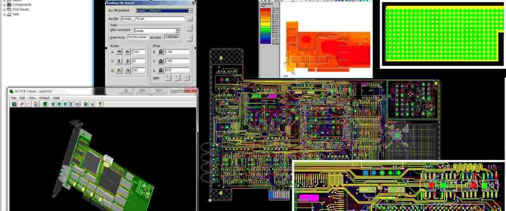
Designers use specialized software to create the PCB layout, which involves placing the components on the board, routing the traces that connect them, and adding power and ground planes. The software can also perform various checks, such as design rule checks (DRCs) and electrical rule checks (ERCs), to ensure that the layout meets the required specifications. With the rapid advancements in technology, the importance of printed circuit layout continues to grow, making it a critical aspect of electronic design.

Basics of Printed Circuit Layout
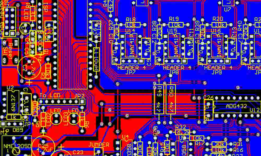
Printed circuit layout refers to the arrangement of components and electrical connections on a printed circuit board (PCB). The layout is a critical aspect of the design process, as it impacts the performance, reliability, and manufacturability of the PCB.
The following are some basic principles to keep in mind when designing a printed circuit layout:
-
Component Placement: The placement of components on the PCB should be carefully considered to ensure optimal performance and ease of assembly. Components should be arranged in a logical and organized manner, with consideration given to their size, shape, and orientation.
-
Trace Routing: Trace routing refers to the routing of electrical connections between components on the PCB. The routing should be designed to minimize signal interference, crosstalk, and noise. The width and spacing of the traces should be carefully selected to ensure proper signal integrity.
-
Grounding: Proper grounding is essential for the performance and reliability of the PCB. The ground plane should be designed to provide a low-impedance path for current return, and should be connected to all ground points on the PCB.
-
Power Distribution: The power distribution network should be designed to provide stable and reliable power to all components on the PCB. The power traces should be designed to minimize voltage drop and noise, and should be routed away from signal traces.
-
Design for Manufacturability: The PCB design should be optimized for ease of manufacturing and assembly. This includes considerations such as component placement, trace routing, and the use of standard PCB sizes and shapes.
By following these basic principles, designers can create printed circuit layouts that are optimized for performance, reliability, and manufacturability.
Factors to Consider in Printed Circuit Layout

When designing a printed circuit board (PCB), there are several factors that must be considered to ensure optimal performance and reliability. In this section, we will discuss some of the key factors that should be taken into account during the printed circuit layout process.
Component Placement
The placement of components on a PCB can have a significant impact on its performance. When placing components, it is important to consider factors such as signal routing, heat dissipation, and accessibility for testing and repair. Components that generate heat, such as power transistors, should be placed in areas with good airflow to prevent overheating. Additionally, components that require high-speed signal routing should be placed in areas with short, direct signal paths to minimize signal loss.
Signal Integrity
Signal integrity is critical to the performance of a PCB. Factors such as trace length, impedance, and crosstalk can all affect signal quality. To ensure good signal integrity, it is important to use proper trace widths and spacing, route signals away from noisy components, and use shielding or isolation where necessary.
Power Integrity
In addition to signal integrity, power integrity is also important for reliable PCB operation. Factors such as voltage drop, ground bounce, and power supply noise can all affect power integrity. To ensure good power integrity, it is important to use proper power and ground planes, minimize voltage drop by using appropriate trace widths, and use decoupling capacitors to filter out noise.
Thermal Management
Thermal management is critical for ensuring that a PCB operates within safe temperature limits. Factors such as component placement, board material, and airflow can all affect thermal performance. To ensure good thermal management, it is important to place heat-generating components in areas with good airflow, use appropriate board materials with good thermal conductivity, and use thermal vias to transfer heat away from components.
In conclusion, when designing a printed circuit board, it is important to consider factors such as component placement, signal integrity, power integrity, and thermal management to ensure optimal performance and reliability.
Designing a Printed Circuit Layout
Designing a printed circuit layout is a crucial step in the manufacturing of electronic devices. The layout determines the physical arrangement of components and their interconnections on the board. A well-designed layout ensures optimal performance, reliability, and manufacturability of the circuit.
To design a printed circuit layout, the following steps are typically followed:
-
Schematic capture: The circuit diagram is created using a schematic capture tool. This tool allows the designer to create a visual representation of the circuit and its components.
-
Component placement: The components are placed on the board according to their function and interconnections. The placement should be optimized for signal integrity, thermal management, and ease of assembly.
-
Routing: The connections between components are routed on the board using traces. The routing should be optimized for signal integrity, impedance control, and EMI/EMC considerations.
-
Design rule check (DRC): The layout is checked against a set of design rules to ensure manufacturability. These rules include minimum trace width and spacing, minimum drill size, and clearance requirements.
-
Gerber generation: The layout is exported in Gerber format, which is a standard file format used by manufacturers to produce the PCB.
When designing a printed circuit layout, it is important to consider the following factors:
-
Signal integrity: The layout should be optimized for signal integrity to minimize noise and distortion.
-
Thermal management: The layout should be optimized for thermal management to prevent overheating of components.
-
Manufacturability: The layout should be optimized for manufacturability to ensure that it can be produced efficiently and reliably.
-
Cost: The layout should be optimized for cost to minimize the overall cost of the circuit.
In conclusion, designing a printed circuit layout is a critical step in the manufacturing of electronic devices. A well-designed layout ensures optimal performance, reliability, and manufacturability of the circuit. By following the steps outlined above and considering the key factors, designers can create high-quality layouts that meet the needs of their applications.
Common Mistakes in Printed Circuit Layout

When designing a printed circuit board (PCB), it is important to avoid common mistakes that can lead to issues with functionality, reliability, and manufacturability. Here are some common mistakes to watch out for:
1. Poor Component Placement
One of the most common mistakes in PCB layout is placing components too close together or in the wrong location. This can lead to signal interference, overheating, and difficulty during assembly. It is important to carefully consider the placement of each component to ensure proper spacing, orientation, and alignment.
2. Inadequate Trace Width and Spacing
Another common mistake is using inadequate trace width and spacing. This can lead to issues with signal integrity, thermal management, and manufacturability. It is important to use appropriate trace widths and spacing based on the current carrying capacity and voltage requirements of the circuit.
3. Improper Grounding
Improper grounding can lead to issues with noise, signal integrity, and EMI/RFI. It is important to properly ground the circuit by connecting all ground pins to a common ground plane and minimizing the loop area of the ground connections.
4. Lack of Design for Manufacturability
Designing a PCB without considering the manufacturing process can lead to issues with yield, cost, and reliability. It is important to consider the capabilities and limitations of the manufacturing process when designing the PCB layout.
5. Inadequate Thermal Management
Inadequate thermal management can lead to issues with overheating and premature failure of components. It is important to properly design the PCB layout to dissipate heat and provide adequate airflow for cooling.
By avoiding these common mistakes in PCB layout, you can ensure a functional, reliable, and manufacturable design.
Advanced Techniques in Printed Circuit Layout
When it comes to designing printed circuits, there are several advanced techniques that can help improve the overall performance of the circuit. Here are a few techniques that can be used:
- Grounding Techniques: Proper grounding is essential for a well-functioning circuit. Advanced grounding techniques include star grounding, ground plane, and split plane grounding.
- Impedance Control: Impedance control is crucial for high-frequency circuits. Advanced techniques for impedance control include controlled impedance routing, differential pair routing, and length matching.
- Signal Integrity: Signal integrity is important for circuits that handle high-speed signals. Advanced techniques for signal integrity include minimizing signal reflections, reducing crosstalk, and using proper termination techniques.
- Power Integrity: Power integrity is essential for circuits that handle high power. Advanced techniques for power integrity include power plane design, decoupling capacitors, and power distribution network analysis.
By implementing these advanced techniques, designers can improve the overall performance of their printed circuits, leading to better signal quality, reduced noise, and improved reliability.

