In the complex world of high-speed electronics, signal integrity is of utmost importance. Ensuring consistent and reliable communication between components is crucial to the overall performance of a system. One key factor affecting signal integrity is impedance control. In this article, we will discuss ten ways to avoid signal integrity problems by effectively managing impedance control in your designs.
Impedance control is essential because inconsistencies in impedance can lead to signal reflection, crosstalk, and timing issues. These problems can have a significant impact on the functionality and performance of a system. To overcome these challenges, designers should be aware of the various techniques and best practices for achieving optimal impedance control.
As we explore these ten methods, it is essential to understand that each design and application is unique and may require a tailored approach. By knowing the potential pitfalls and implementing these strategies, you will be better prepared to achieve a well-designed system with minimal signal integrity issues.
Understanding Impedance Control
Impedance Basics
Impedance is a measure of how much a circuit resists the flow of an alternating current (AC) signal. It depends on the characteristics of the materials used in a PCB, such as the dielectric constant and the geometry of the traces. Impedance control in PCB design is necessary to ensure the signals reach their destination with minimal distortion, noise, and interference.
Impedance matching is essential because any sudden changes in impedance can cause signal reflections. These reflections lead to signal integrity issues like ringing, overshoot, and timing issues. To maintain a constant impedance, it is crucial to consider trace width, trace spacing, and dielectric thickness while designing a PCB.
Effects on Signal Integrity
Several factors can impact signal integrity in impedance-controlled PCBs:
-
Mismatched impedance: If the components and traces on a PCB have different impedances, reflections and distortion can occur, which negatively affect signal quality.
-
Signal crosstalk: When signals on adjacent traces couple electromagnetically, the resulting interference can disrupt data transmission.
-
High-frequency components: As the frequency of signals increase, their sensitivity to impedance mismatches also increases. This sensitivity makes impedance control a necessity for high-speed designs.
In summary, impedance control is vital in maintaining signal integrity in printed circuit boards. By understanding the basics of impedance and taking steps to mitigate its negative effects, you can create more reliable and efficient PCB designs.
PCB Design Guidelines for Impedance Control
Proper Stack-Up
A well-designed stack-up is crucial for impedance control. It provides a controlled impedance environment, minimizing signal reflections and crosstalk. Consider the following points when designing your stack-up:
- Use a symmetrical structure to maintain a balanced impedance.
- Place high-speed signal layers as close as possible to adjacent ground or power planes.
- Utilize the same dielectric materials and thickness, ensuring consistent impedance throughout the layers.
Trace Width and Spacing
Selecting the appropriate trace width and spacing is vital for maintaining controlled impedance. Here are some guidelines:
- Use a trace width calculator or field solver to determine the correct width for a target impedance value.
- Maintain a consistent spacing between traces to avoid impedance mismatches and crosstalk.
- Consider using differential pairs for high-speed signals, as they can help maintain constant impedance.
Following these guidelines ensures that your PCB design has controlled impedance, reducing signal integrity problems and improving overall performance.
Use of Simulation Tools

Pre-Layout Simulation
Before designing a PCB layout, using simulation tools to predict the possible signal integrity issues is crucial. Pre-layout simulation tools can help identify potential issues that may arise during the design process. They can provide valuable insights into the impedance control, allowing you to make necessary adjustments before the design stage. Some popular pre-layout simulation tools include:
Utilizing these tools enables you to model and analyze signal paths, ensuring the design specifications are met.
Post-Layout Simulation
After completing the PCB layout, it is essential to perform post-layout simulation to evaluate signal integrity and verify that all design requirements have been met. Post-layout simulation tools can identify if any impedance control problems have been introduced during layout or if design changes are needed. Some commonly used post-layout simulation tools are:
- Cadence Allegro Sigrity PI
- Mentor Graphics HyperLynx (with Signal Integrity and Power Integrity analysis)
- Ansys SIwave
These tools allow you to validate the performance of your design, ensuring that it meets the target impedance values and industry standards. Additionally, post-layout simulation can minimize the risk of unnecessary redesigns, saving both time and resources.
Making use of both pre- and post-layout simulation tools is an effective way to ensure a robust, high-performance design that avoids signal integrity issues through impedance control. Remember that it is crucial to consider factors like material properties, trace dimensions, and interconnect designs when utilizing these tools to optimize the PCB layout.
Material Selection
Dielectric Constant
The dielectric constant (Dk) is an essential property of the PCB material and has a significant impact on signal integrity. Selecting materials with an appropriate dielectric constant is crucial to minimize signal reflection and attenuation when designing high-speed circuits. Here’s a list of common materials and their associated Dk values:
- FR-4: 4.0 – 4.8
- Rogers 3003: 3.0
- Rogers 4003/4350: 3.48
PCB designers should consider the specific Dk value suitable for their application to avoid impedance mismatches that might lead to signal integrity problems.
Loss Tangent
Another vital material property to consider is the loss tangent (tanδ), which represents the energy dissipation within the dielectric material. A lower loss tangent reduces signal losses and helps maintain signal quality in high-speed digital and RF designs. Here are some typical loss tangent values for commonly used materials:
- FR-4: 0.020
- Rogers 3003: 0.001
- Rogers 4003/4350: 0.0035
It’s essential to choose materials with suitable loss tangent values based on the desired electrical performance and signal integrity. Be aware of the trade-off between cost and performance, as high-performance materials may be more expensive than standard ones.
Managing Return Paths
Proper management of return paths is essential for maintaining signal integrity in high-speed PCB designs. In this section, we will discuss two key techniques to effectively manage return paths: Ground Planes and Stitching Capacitors.
Ground Planes
A ground plane is a continuous conductive layer, often made of copper, that serves as the reference plane for return currents. It is crucial in maintaining low impedance for return paths, which helps to minimize signal reflections, noise, and other signal integrity issues. Key points to consider when designing ground planes are:
- Use continuous ground planes: This helps to ensure a low impedance path for return currents, thus reducing signal noise and reflections.
- Avoid ground loops: Ensure there are no loops in the ground plane, as they can create unintended signal coupling.
- Place ground planes as close as possible to signal layers: This minimizes the loop area between signals and return paths, reducing unwanted inductance and electromagnetic interference (EMI).
Stitching Capacitors
Stitching capacitors are used to connect power and ground planes across different PCB layers, providing low impedance return paths for signals. By using stitching capacitors, it is possible to maintain signal integrity even when signals traverse between different layers. Consider the following tips when utilizing stitching capacitors in your design:
- Place capacitors close to vias: This reduces the inductive loop area and helps maintain low impedance paths.
- Use multiple stitching capacitors: Distributing multiple capacitors across the design can reduce the overall impedance, improving signal integrity.
- Select appropriate capacitance values: Be sure to choose capacitors with values suited for the target frequency range to ensure effective low impedance paths.
By implementing these techniques, you can effectively manage return paths in your PCB designs, helping to maintain signal integrity and avoid potential issues related to impedance control.
Termination Techniques
Series Termination
Series termination is a simple and cost-effective method for controlling signal integrity. This technique involves placing a resistor (Rs) in series with the signal line, close to the driver. The resistor value is chosen to match the characteristic impedance (Z0) of the transmission line, minimizing reflections.
- Select an appropriate resistor value depending on the transmission line impedance.
- Place the resistor near the driver to minimize signal discontinuities.
- Ensure proper grounding of the transmission line to reduce noise.
Parallel Termination
Parallel termination is another effective method for managing signal integrity. It utilizes a resistor (Rp) connected in parallel to the transmission line, at the receiving end. This resistor should also match the characteristic impedance of the transmission line.
- Choose a resistor value that matches the transmission line impedance.
- Connect the resistor at the receiving end to absorb reflected signals.
- Ensure proper connections and grounding to minimize noise.
By employing these termination techniques, you can successfully mitigate signal integrity issues resulting from impedance mismatches. Both series and parallel termination methods have their advantages and should be chosen based on specific design requirements to achieve optimal results.
Handling High-Speed Signals
Differential Signaling
Differential signaling is a technique used for effectively transmitting high-speed signals. It involves sending two complementary signals on separate traces, typically referred to as the positive (_P) and negative (_N) signals. The receiver takes the difference between these two signals, which results in noise reduction and improved signal integrity. To correctly implement differential signaling:
- Ensure correct termination: Use appropriate termination impedance to minimize reflections.
- Route traces close together: Maintain a consistent distance between the traces to minimize crosstalk and maintain consistent impedance.
- Minimize length deviation: Keep the length difference between the _P and _N signals to a minimum in order to maintain good signal quality.
Length Matching
High-speed signals can be sensitive to timing mismatches caused by differences in trace length. To prevent this, it is essential to match the lengths of critical signal paths, particularly when dealing with differential signaling, data, and clock lines. When handling high-speed signals, follow these best practices for length matching:
| Signal Type | Maximum Length Mismatch |
|---|---|
| Data | 10% of Unit Interval |
| Clock | 5% of Unit Interval |
| Differential | 2% of Unit Interval |
- Use corners and curves: Adjust the trace path using corners and curves to increase length without causing impedance discontinuities.
- Utilize delay tuning patterns: Add serpentine traces in situations where fine-tuning of length is required.
- Consider manufacturing tolerances: Allow some margin for error due to manufacturing tolerances when following strict length matching guidelines.
By implementing differential signaling and length matching best practices, engineers can more easily avoid signal integrity problems in high-speed circuits and ensure optimal performance.
Mitigating Crosstalk and EMI
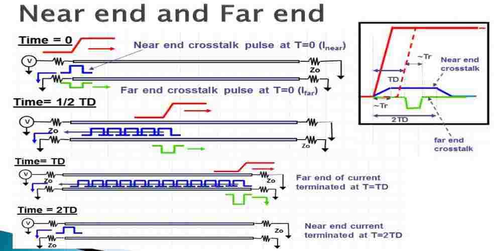
Coupling Mechanisms
Crosstalk and Electromagnetic Interference (EMI) occur when unwanted signals couple into adjacent traces or cables. This can lead to signal degradation and ultimately result in errors. Understanding and mitigating these coupling mechanisms is essential to ensure signal integrity.
There are three primary coupling mechanisms to consider:
- Capacitive coupling: Occurs when two conductors are separated by an insulating medium, creating an electric field that causes signal coupling. To reduce capacitive coupling, increase the distance between conductors or reduce the trace width.
- Inductive coupling: Occurs when changing magnetic fields from one conductor induce voltage in a nearby conductor. To minimize inductive coupling, align traces orthogonally and avoid running parallel traces close together.
- Radiative coupling: Occurs when a conductor emits electromagnetic waves that are picked up by nearby conductors. This can be reduced by using smaller loops and decreasing the trace length.
Shielding Strategies
Shielding is an important technique to mitigate crosstalk and EMI. It involves enclosing conductors or components with a conductive or magnetic material to block interference. Here are some strategies to consider implementing:
- Ground planes: A continuous ground plane under the signal layer can help to shield against capacitive and radiative coupling. It also provides a low-impedance return path for return currents.
- Guard traces: These are traces running parallel to signal traces, connected to the ground. Guard traces help to reduce crosstalk and provide an alternative path for return currents.
- Conductive shielding: Encasing sensitive components or sections of a PCB in a conductive material, like copper, can block electromagnetic radiation and alleviate EMI.
- Magnetic shielding: Applying ferromagnetic materials around sensitive components can help to attenuate magnetic field interference.
When designing a PCB, always consider the potential impact of crosstalk and EMI on signal integrity. By understanding coupling mechanisms and implementing appropriate shielding strategies, you can optimize board layout and ensure signal integrity in your designs.
Inspecting and Testing PCBs
One of the key aspects of maintaining signal integrity in PCBs is to ensure that the boards are properly inspected and tested.
Time Domain Reflectometry
Time Domain Reflectometry (TDR) is a powerful technique for verifying impedance control. A TDR test can help identify impedance mismatches and discontinuities in the transmission lines. The following steps can be taken to conduct a TDR test:
- Prepare the TDR test setup, which includes connecting the TDR instrument to the Device Under Test (DUT).
- Set up the correct parameters to analyze the DUT, such as time resolution (rise time), frequency range, and impedance.
- Run the test and analyze the results in terms of reflections, losses, and impedance values.
It is essential to perform TDR testing to ensure signal integrity throughout the PCB.
Visual Inspection and Testing
Visual inspection of a PCB can reveal potential signal integrity issues, such as poor soldering, misaligned components, or damaged traces. Here are some points to consider during visual inspection and testing.
- Examine the PCB for any visible damage or contamination that could compromise signal integrity.
- Check component alignment to ensure proper connectivity and, in turn, minimize impedance mismatch.
- Ensure proper soldering quality and avoid any issues like cold joints or excess solder due to solder bridging.
- Use magnification and illumination tools (as needed) to assist in the inspection process.
Regular visual inspection and testing can help maintain signal integrity by detecting potential problems early on and allowing corrective measures to be taken.
