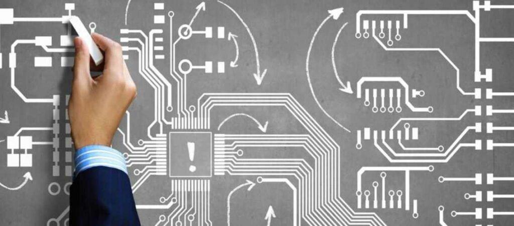
Switching power supply PCB design is an essential aspect of creating efficient and reliable power supplies. The design of a switching power supply PCB determines the performance of the power supply, as well as its size, cost, and reliability. A well-designed PCB can help to minimize electromagnetic interference (EMI), reduce power losses, and improve the overall efficiency of the power supply.
One of the most critical factors in switching power supply PCB design is the layout of the components. The layout of the components should be optimized to minimize the length of the traces and reduce the amount of noise and interference. The placement of the components should be carefully planned to ensure that the power supply operates efficiently and reliably. Additionally, the choice of components, such as capacitors and inductors, can have a significant impact on the performance of the power supply.
Basics of Switching Power Supply PCB Design
Switching power supply PCB design is a critical aspect of power supply design. A well-designed PCB can help to minimize EMI and improve efficiency. Here are some basics to keep in mind when designing a switching power supply PCB:
-
Component Placement: The placement of components on the PCB is crucial for the performance of the power supply. It is important to place the components in a way that minimizes the length of the traces and reduces the loop area. This can help to minimize EMI and improve the efficiency of the power supply.
-
Ground Planes: Ground planes are an essential part of a switching power supply PCB design. They can help to reduce the impedance of the ground connection and minimize EMI. It is important to have a solid ground plane that is connected to the chassis ground.
-
Trace Width: The width of the traces on the PCB is critical for the performance of the power supply. A trace that is too narrow can cause voltage drops and reduce the efficiency of the power supply. It is important to use the appropriate trace width for the current that will be flowing through the trace.
-
Thermal Management: Switching power supplies can generate a lot of heat. It is important to design the PCB in a way that allows for effective thermal management. This can include using copper pours, thermal vias, and heatsinks.
-
EMI Filtering: EMI filtering is an important consideration when designing a switching power supply PCB. It is important to include EMI filters on the input and output of the power supply to reduce the amount of noise that is generated.
By keeping these basics in mind, you can design a switching power supply PCB that is efficient, reliable, and minimizes EMI.
Power Supply Topologies

When it comes to designing a power supply, there are several topologies to choose from. Each topology has its advantages and disadvantages, and the choice of topology will depend on the specific requirements of the application. In this section, we will discuss the three most common power supply topologies: Buck Converter, Boost Converter, and Buck-Boost Converter.
Buck Converter
A Buck Converter is a step-down converter that converts a higher voltage to a lower voltage. It is widely used in applications where a constant output voltage is required, such as in laptops, mobile phones, and other electronic devices. The Buck Converter is efficient and relatively simple to design, making it a popular choice for many applications.
The operation of a Buck Converter is based on the principle of inductor current flow. When the input voltage is applied, the inductor stores energy in its magnetic field. When the switch is turned off, the energy stored in the inductor is transferred to the output capacitor, resulting in a lower output voltage.
Boost Converter
A Boost Converter is a step-up converter that converts a lower voltage to a higher voltage. It is commonly used in applications where a higher output voltage is required, such as in LED lighting and battery-powered devices. The Boost Converter is relatively simple to design and has a high efficiency, making it a popular choice for many applications.
The Boost Converter operates on the principle of inductor current flow, similar to the Buck Converter. When the input voltage is applied, the inductor stores energy in its magnetic field. When the switch is turned off, the energy stored in the inductor is transferred to the output capacitor, resulting in a higher output voltage.
Buck-Boost Converter
A Buck-Boost Converter is a combination of the Buck and Boost Converters. It can be used to convert a higher voltage to a lower voltage or a lower voltage to a higher voltage. It is commonly used in applications where the input voltage may vary, such as in automotive and solar applications.
The Buck-Boost Converter operates on the principle of inductor current flow, similar to the Buck and Boost Converters. When the input voltage is applied, the inductor stores energy in its magnetic field. When the switch is turned off, the energy stored in the inductor is transferred to the output capacitor, resulting in a higher or lower output voltage depending on the application.
In conclusion, the choice of power supply topology will depend on the specific requirements of the application. Each topology has its advantages and disadvantages, and careful consideration should be given to the design of the power supply to ensure optimal performance and efficiency.
PCB Layout Guidelines
When designing a switching power supply PCB, it is important to follow certain guidelines to ensure proper function and reliability. Here are some key considerations for PCB layout:
Component Placement
The placement of components on the PCB can have a significant impact on the performance of the switching power supply. To ensure proper operation, it is important to follow these guidelines:
- Place components as close to the IC as possible to minimize trace length and reduce noise.
- Keep high-voltage components away from low-voltage components to prevent interference.
- Group components based on their function to simplify trace routing and reduce noise.
Trace Routing
Trace routing is an important aspect of PCB layout for switching power supplies. Here are some guidelines to follow:
- Keep traces as short and direct as possible to minimize resistance and inductance.
- Use wide traces for high-current paths to reduce voltage drop and heat dissipation.
- Keep traces away from high-voltage components to prevent arcing.
Grounding
Proper grounding is critical for the performance and reliability of a switching power supply. Follow these guidelines:
- Use a dedicated ground plane to reduce noise and interference.
- Connect the ground plane to the chassis to prevent ground loops.
- Keep the ground plane as close to the power components as possible to reduce noise.
Decoupling Capacitors
Decoupling capacitors are used to filter out noise and provide stable power to the switching power supply. Here are some guidelines to follow:
- Place decoupling capacitors as close to the IC as possible to minimize trace length.
- Use multiple capacitors of different values to filter out a range of frequencies.
- Use low-ESR (Equivalent Series Resistance) capacitors for best performance.
By following these guidelines, you can ensure a reliable and well-performing switching power supply PCB layout.
Thermal Management
Thermal management is an important aspect of switching power supply PCB design. It involves the dissipation of heat generated by the power supply components during operation. If the heat generated is not properly dissipated, it can cause damage to the components and lead to the failure of the power supply.
There are several ways to manage thermal issues in switching power supply PCB design. One of the most common methods is the use of heat sinks. Heat sinks are devices that are designed to absorb and dissipate heat away from the components. They are typically made of materials with high thermal conductivity, such as aluminum or copper.
Another way to manage thermal issues is through the use of thermal vias. Thermal vias are small holes that are drilled through the PCB to allow heat to escape from the components. They are filled with a thermally conductive material, such as copper, to enhance heat dissipation.
In addition to heat sinks and thermal vias, proper component placement can also help manage thermal issues. Components that generate a lot of heat, such as power transistors, should be placed in areas of the PCB with good airflow. This can help dissipate heat away from the components.
It is important to note that while thermal management is critical to the proper operation of switching power supplies, it is not a one-size-fits-all solution. The specific thermal management techniques used will depend on the specific design requirements and operating conditions of the power supply. Careful consideration should be given to the thermal management strategy during the design phase to ensure proper operation and reliability of the power supply.
EMI/EMC Considerations
When designing a switching power supply PCB, it is important to consider EMI (Electromagnetic Interference) and EMC (Electromagnetic Compatibility) issues. EMI occurs when electromagnetic radiation from the power supply interferes with other electronic devices, while EMC refers to the ability of the power supply to operate in a shared electromagnetic environment without causing interference.
To minimize EMI and ensure EMC compliance, the following considerations should be taken into account:
-
Layout: Proper layout is crucial for minimizing EMI. The power supply should be placed as far away as possible from other sensitive electronics, and traces carrying high-frequency signals should be kept as short as possible. Ground planes should be used to provide a low-impedance return path for high-frequency currents.
-
Filtering: The use of filters can help reduce EMI. Common mode chokes, ferrite beads, and capacitors can be used to attenuate high-frequency noise and filter out unwanted signals.
-
Shielding: Shielding can be used to prevent EMI from escaping the power supply. Conductive enclosures, metal shields, and EMI gaskets can be used to block electromagnetic radiation.
-
Component Selection: The selection of components can also affect EMI. Low ESR (Equivalent Series Resistance) capacitors should be used to minimize voltage spikes, and high-quality inductors should be used to reduce noise.
By taking these considerations into account, designers can ensure that their switching power supply PCBs meet EMI/EMC standards and operate reliably in a shared electromagnetic environment.
Testing and Troubleshooting

After designing a switching power supply PCB, it is essential to test it thoroughly before putting it into production. Testing helps to identify any design flaws or manufacturing defects that may affect the performance of the power supply. Troubleshooting is also necessary to diagnose and fix any issues that may arise during testing or later in the field.
One of the critical parameters to test is the output voltage. The output voltage should be within the specified range, and any deviation should be minimal. A multimeter can be used to measure the output voltage accurately. Other parameters to test include the input voltage, output current, and efficiency.
It is also essential to check for any abnormal behavior during testing. For example, if the power supply produces noise or overheats, it could indicate a design flaw or a manufacturing defect. In such cases, the power supply should be further tested and analyzed to identify the root cause of the problem.
Troubleshooting is necessary to diagnose and fix any issues that may arise during testing or later in the field. Troubleshooting involves identifying the symptoms, analyzing the possible causes, and testing the power supply to confirm the cause of the problem.
A systematic approach to troubleshooting can save time and effort. It is recommended to start with the most likely cause of the problem and work through a list of possible causes until the issue is resolved. Common causes of power supply issues include faulty components, poor soldering, incorrect wiring, and design flaws.
In conclusion, testing and troubleshooting are critical steps in switching power supply PCB design. Thorough testing can identify any design flaws or manufacturing defects, while troubleshooting can help diagnose and fix any issues that may arise during testing or later in the field.
