Top layer PCB is a type of printed circuit board that is commonly used in electronic devices. It is the topmost layer of a multi-layer PCB and contains the majority of the components and circuitry. The top layer is responsible for routing the signals between the components and connecting them to the other layers of the board.
One of the main advantages of using a top layer PCB is that it allows for a more compact design. By placing the majority of the components on the top layer, the board can be made smaller and more efficient. This is particularly important in devices where space is limited, such as smartphones and wearables.
Another advantage of top layer PCBs is that they are easier to manufacture than other types of PCBs. Because the top layer contains the majority of the components, the process of placing and soldering the components is simplified. This can result in a faster and more cost-effective manufacturing process, which is important for companies that need to produce large quantities of electronic devices.
What is a Top Layer PCB?
Definition
A top layer PCB, also known as a top-side PCB, is a printed circuit board that has conductive traces and components mounted on the top layer of the board. It is one of the most common types of PCBs used in electronic devices, as it allows for easy access to the components and is ideal for high-density designs.
Functionality
The top layer of a PCB is responsible for carrying most of the electrical signals and power between the components. It is also where the majority of the components are mounted, including resistors, capacitors, and integrated circuits. The top layer is typically covered with a layer of solder mask to protect the traces and components from damage.
One of the main advantages of a top layer PCB is that it allows for easy access to the components during assembly and testing. This makes it easier to troubleshoot and repair any issues that may arise during the manufacturing process.
Additionally, top layer PCBs are ideal for high-density designs, as they allow for a large number of components to be mounted in a small space. This is particularly useful in applications such as mobile devices, where space is at a premium.
Overall, top layer PCBs are a versatile and widely used type of printed circuit board that offer a range of benefits for electronic device manufacturers.
Design Considerations
When designing a top layer PCB, there are several important considerations to keep in mind to ensure optimal performance and reliability. Here are some key design considerations to take into account:
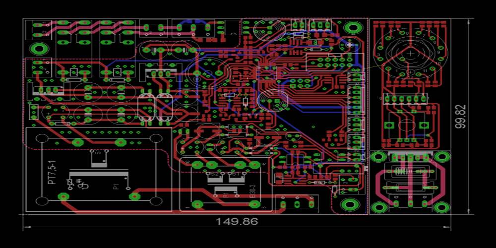
Trace Width and Spacing
Trace width and spacing are crucial aspects of PCB design that can significantly impact the performance of the board. The width and spacing of traces should be chosen based on the current carrying capacity and voltage drop requirements of the circuit. Narrow traces can lead to high resistance, which can cause voltage drop and heat dissipation issues.
A trace width calculator can be used to determine the optimal trace width for a given current and copper weight. It is also important to consider the spacing between traces, as it can affect the potential for crosstalk and signal integrity issues.
Via Placement
Via placement is another important consideration in top layer PCB design. Vias are used to connect different layers of the board together and allow for the transfer of signals and power. The placement of vias can impact the performance of the board, with improper placement potentially leading to signal degradation and interference.
To minimize signal interference and ensure optimal performance, vias should be placed in areas of the board where they will not interfere with critical traces or components. It is also important to consider the size and placement of the via pads, as they can affect the reliability and manufacturability of the board.
Copper Weight
The copper weight of a PCB refers to the thickness of the copper layer on the board. The copper weight directly affects the current carrying capacity of the board, with heavier copper allowing for higher current loads. However, heavier copper can also increase the cost and complexity of the manufacturing process.
When choosing the copper weight for a top layer PCB, it is important to consider the current requirements of the circuit and balance them with the cost and manufacturability of the board. A copper weight calculator can be used to determine the optimal copper weight for a given current and trace width.
In summary, designing a top layer PCB requires careful consideration of trace width and spacing, via placement, and copper weight. By taking these factors into account, designers can ensure optimal performance, reliability, and manufacturability of their boards.
Materials Used in Top Layer PCBs

When it comes to designing and manufacturing top layer PCBs, there are several materials that are commonly used. These materials play a crucial role in determining the overall quality, performance, and durability of the PCB. In this section, we’ll take a closer look at some of the most important materials used in top layer PCBs.
Copper Clad Laminate
Copper clad laminate is one of the most important materials used in top layer PCBs. It is a composite material that consists of a layer of copper foil bonded to a substrate. The substrate can be made of various materials, including fiberglass, paper, or a combination of both. The thickness of the copper foil can vary depending on the application, but it is typically between 0.5 and 4 ounces per square foot.
Soldermask
Soldermask is another important material used in top layer PCBs. It is a layer of polymer that is applied to the surface of the PCB to protect the copper traces from oxidation and to prevent solder from bridging between adjacent pads. Soldermask is typically green in color, but it can also be black, white, or any other color depending on the requirements of the application.
Silkscreen
Silkscreen is a layer of ink that is applied to the surface of the PCB to provide labeling and identification. It is typically white in color and is used to mark component locations, pin numbers, and other important information. Silkscreen can also be used to add logos or other decorative elements to the PCB.
In conclusion, the materials used in top layer PCBs are critical to their performance and durability. Copper clad laminate, soldermask, and silkscreen are just a few of the materials that play a crucial role in the design and manufacturing of top layer PCBs. By understanding the properties and characteristics of these materials, designers and manufacturers can create high-quality and reliable PCBs that meet the needs of their customers.
Manufacturing Process
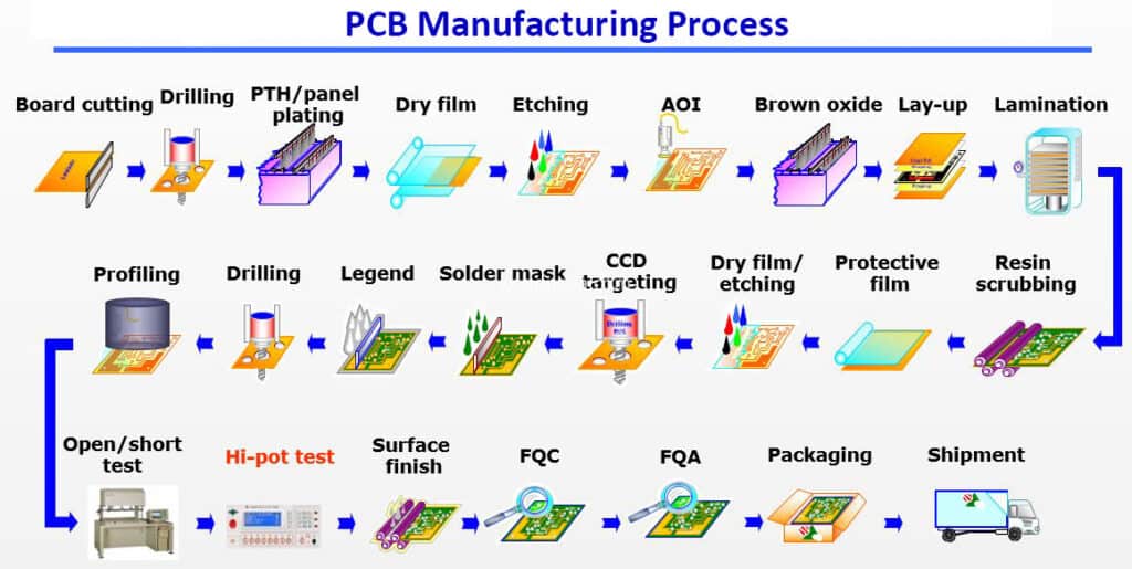
The manufacturing process of top layer PCB involves several steps, including etching, drilling and plating, soldermask, and silkscreen.
Etching
Etching is the process of removing the unwanted copper from the PCB surface. This is done by applying a chemical solution to the surface, which reacts with the copper and dissolves it. The remaining copper forms the circuit traces.
Drilling and Plating
After etching, the PCB is drilled to create holes for components and connections. The holes are then plated with a thin layer of copper to create a conductive path between the top and bottom layers of the PCB.
Soldermask
Soldermask is a layer of polymer applied to the PCB surface to protect the copper traces from oxidation and to prevent accidental solder bridging during assembly. The soldermask is applied using a screen-printing process and can be any color.
Silkscreen
Silkscreen is a layer of ink applied to the PCB surface to provide labeling and identification for components and connectors. The silkscreen is applied using a screen-printing process and can be any color.
Overall, the manufacturing process of top layer PCBs involves several steps that require precision and accuracy to ensure high-quality and reliable circuit boards.
Advantages of Top Layer PCBs
Cost-effective
One of the biggest advantages of top layer PCBs is that they are cost-effective. As the name suggests, these PCBs have all their components on the top layer, which makes them easier and cheaper to manufacture. The manufacturing process for top layer PCBs is simpler and requires fewer materials, which means that they are less expensive than other types of PCBs.
High Reliability
Top layer PCBs are also highly reliable. Because all the components are on the top layer, it is easier to test and inspect the PCB for any defects or issues. This means that any problems can be identified and fixed quickly, which reduces the risk of failure and increases the reliability of the PCB.
Easy to Repair
Another advantage of top layer PCBs is that they are easy to repair. Because all the components are on the top layer, it is easy to access them and replace any faulty or damaged components. This means that any repairs can be done quickly and easily, which reduces downtime and increases the lifespan of the PCB.
In summary, top layer PCBs are cost-effective, highly reliable, and easy to repair. These advantages make them a popular choice for many applications, including consumer electronics, industrial equipment, and medical devices.
Disadvantages of Top Layer PCBs
Limited Layer Count
One of the main disadvantages of using top layer PCBs is the limited layer count. Top layer PCBs are typically limited to only two layers, which can limit the complexity and functionality of the circuit. This is because the top layer is used for routing signals, while the bottom layer is used for ground and power planes. If more layers are needed, a different type of PCB may be required.
Limited Routing Options
Another disadvantage of top layer PCBs is the limited routing options. With only two layers available, the routing options can be limited, making it difficult to design certain types of circuits. This can be especially problematic for high-density designs or circuits with complex routing requirements.
Susceptibility to EMI
Top layer PCBs are also more susceptible to electromagnetic interference (EMI) than other types of PCBs. This is because the top layer is exposed and not shielded by other layers. EMI can cause interference with the signals on the PCB, leading to errors or malfunctions in the circuit. To mitigate this issue, additional shielding may be required, which can add complexity and cost to the design.
In summary, while top layer PCBs have their advantages, such as ease of design and lower cost, they also have some significant drawbacks. These include limited layer count, limited routing options, and susceptibility to EMI. When designing a circuit, it’s important to weigh the pros and cons of different PCB types to ensure the best possible performance and reliability.
