You, like most of us, probably understand the importance of printed circuit boards to electronics. However, a lot of misconceptions exist in this sphere, especially for electronic students or enthusiasts. Firstly, does the term printed wiring board and the printed circuit board mean the same thing? If different, then what makes up the difference? Even the most astute electronic enthusiast can confuse these terms. But luckily for you, this article will canvass all the areas about the printed wiring board. Are you getting ahead of yourself already? Please don’t.
What is a Printed Wiring Board?
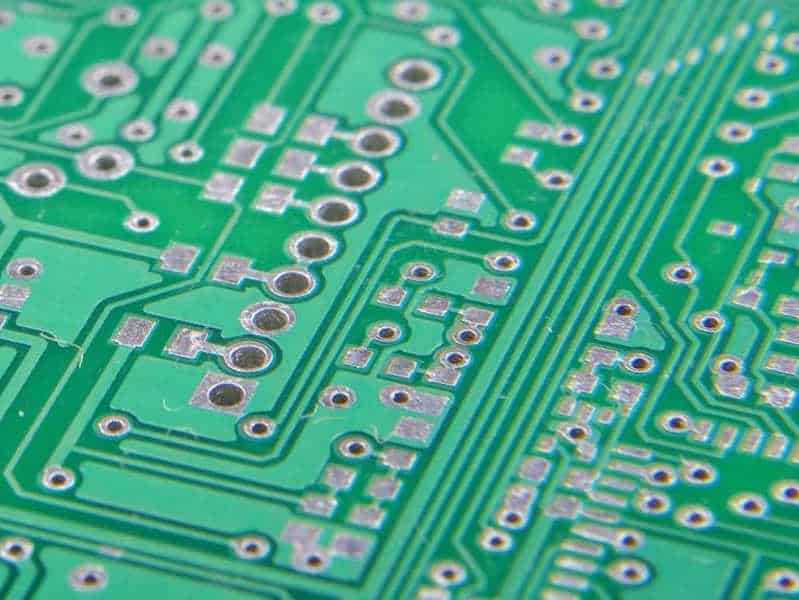
One of the most vital aspects to understand first about a PWB (printed wiring board) entails its definition. The PWB stands for printed wiring board and contains an epoxy glass resin or substrate that creates interconnection. It also attaches PCB elements to realize a circuity that proves helpful in developing electronic devices.
We achieve the printed wiring board manufacturing through an etching process to expose conduction-insulating surfaces between conduction-enabling traces. It becomes impossible for you to develop efficient and present-day electronics without quality PWBs. We can interchangeably use the term printed wiring board and printed circuit board when it comes to electronics. However, subtle differences exist for the keen. Therefore, the two terms refer to two different things, though the differences can prove subtle.
You will most likely note the divergent uses of the term printed wiring board and printed circuit board based on several factors. For instance, the geographical location can determine the preference for PWB or PCB. The electronics industry in Japan predominantly uses PWB or printed wiring boards, whereas the electronics industry in the USA prefers printed circuit boards or PCBs.
Officially, no correct term exists between the two. However, let us look at the definitions based on the different industry outlooks.
Request Printed Wiring Board Quote, Pls send PCB Files to Sales@raypcb.com Now
Industry Definition of a Printed Wiring Board
At the industry level, both the PWB and the PCB emphasize the circuit board wiring though the definition differ lightly. For instance, the SMTA defines the printed wiring board as a substrate mainly composed of epoxy glass deployed in providing interconnections and lands for component attachment in establishing a functional electronic circuit.
On the other hand, a PCB emphasizes the multilayer, sideways, and width relationships of the conductor run in effecting the circuity in a specific way as designed. It transcends the point-to-point connections otherwise emphasized by a PWB. You, therefore, find subtle differences in the emphasis, especially the completeness of the circuit.
Uses
The deployment of the term PWB and PCB also differ based on your geographical location. The way you refer to a PEC or a printed electronic circuit) in the US electronic industry proves different from what the electronic circuit industry in Japan, for instance, prefers. In the United States, most industry players prefer using PCB to refer to printed circuits. In Japan, the term PWB or printed wiring board gets preferred. However, in this instance, the two often infer the same thing – printed electronic circuits. Therefore, you can always decide to use a PWB or PCB based on your preference while also considering the insights provided.
Difference between a Printed Wiring Board (PWB) and a Printed Circuit Board (PCB)
Is there a difference between a PWB and a PCB? Well, the printed wiring board implies the development of an electrical circuit or network within a substrate. We typically furnish the connection on etched conductive plates, while attaching the electronic components in making it a functional circuit.
Conversely, a printed circuit board (PCB) offers the electronic components the physical support needed and connects them electronically. The formation of electrical paths, also called traces, happens through etching. You will find the traces running across the surface of the board. It can also get furnished on multiple layers and connected or linked through vias. As a result, a PCB more or less comes as a populated printed wiring board. PCBs function through the existence of the composition of their components. Because of this, when you alter electronic component composition on the PCB wiring or circuitry changes its performance.
How can You Make a Printed Wiring Board?
If you want a PWB, then understanding its development process becomes essential. We develop printed wiring boards from a series of divergent fabrication processes. It entails the application of equipment and materials to see the project complete successfully. You, therefore, will have to follow the following steps when making it as a DIY venture or understand them when contracting an external manufacturing company like RayMing PCB and Assembly.
Lamination
As in most cases, lamination encompasses the combination of the substrate layers under pressure and heat to establish laminates. The substrates come as dielectric material and can include ceramic, FR4, etc., which gives the conductive layers, the needed electrical isolation. Conversely, Prepreg comes as resin-based materials that hold the laminated parts together. As a result, it is always unsurprising to find the Prepreg and the substrate layers sandwiched during lamination.
Drilling
You cannot fix components on the printed wiring board without boring holes into the board. You achieve this through a drilling process, upon which vias and components get fixed. The drilling process can happen automatically or through a manual process, depending on your capacity. However, each utilizes a distinct set of equipment and machines. In most cases, you generate the drill file by using the Gerber file. It provides you with the locations of the drill holes on the bard.
If you plan and want to conduct the plated through-hole assembly, then manual drilling using a human-operated machine can get deployed. It requires drill bits of the correct size to enable the boring of the fitting hole sizes. However, for the automatic drilling process, special and programmed automatic machines use the drill files in boring the required holes (of the desired parameters). Automated drilling approaches can come in various forms through laser drilling proves the dominant one. The bored holes become instrumental for the printed wiring assembly process that follows later on.
Conductive Track Creation
Every form of a printed wiring board relies on the conductive track to transmit the required electrical signal. As a result, you cannot underestimate the need to create this signal path properly. In most instances, the typical material used for the conductive trace comes as copper. It is readily available and has an admirable signal transfer or transmission qualities. You can consistently achieve this through subtractive or additive methods.
In the additive approach, you deposit the copper on the surface of the substrate in line with the desired pattern. On the other hand, you apply the etched copper film to remove unwanted material in the subtractive approach. From this point, you will have the desired pattern of the conductive path.
What Materials do You Use in the Printed Wiring Board Fabrication?

You need different materials when it comes to the development of a printed wiring circuit. A PWB contains different parts, which in turn need separate sets of materials. However, you can use the same materials you deploy in fabricating a printed wiring board to a printed circuit board. Nonetheless, the material types depend on the type of application the board will get subjected to.
You can segment a PWB into two major parts, the bare PWB wiring board, and the PCB wiring elements. The bare board contains the non-conductive layers and the conductive layers. You use the conductive layer for signal transfer, whereas the non-conductive segment are good for electrical insulation or isolation. PCB wiring materials commonly used as the PWB conductive layer include gold, silver, and copper.
Gold possesses the utmost levels of conductivity besides the least electrical resistance. However, it’s costly and thus rarely used. However, you will find copper as the most popular for printed wiring. The conducting layer is instrumental in furnishing the signal transfer path for the printed wiring board and PCBs. Conversely, the non-conducting layer, primarily composed of low electrical transference capacity, are appropriate for insulation purposes. It can come as a composite epoxy substrate, FR4, ceramic, etc. But you must understand that each non-conducting material possesses distinct thermal conductance and insulation properties. Because of this, you will always find the FR4 material as the most popular type used with multiple variants to supplement its dielectric attributes.
You will probably not miss other typical materials like the Prepreg, which becomes instrumental in holding the different layers together. It comes as fiberglass pre-impregnated with epoxy resin. The last one entails the solder, which fixes the solder joints in place.
Can Conformal Coating Work on Printed Wiring Boards?
The conformal coating comes as a resin-based coat or layer that you apply on a populated printed circuit board to shield it from undesired external elements. Such elements include moisture, dust, spillage, and other external conditions that make the PWB deteriorate. Conformal coatings attach to the surface and take up the PCB board’s form. However, it mainly applies to populated boards, which proves the opposite for a printed wiring board. PWBs come unpopulated and thus unsuitable with the conformal coating when it comes to its development. Additionally, the absence of features on a printed wiring board’s surface means a lack of aspects that require protection from environmental or external elements.
What Types of Surface Finishes Can Apply on Printed Wiring Boards and PCBs?
If you want surface finishes for both printed circuit boards and printed wiring boards, it helps to consider those that can work for both the PWB and the PCB without problems. Surface finishes prove protective and we can often apply them on top of the traces of a printed wiring board. It thus becomes unsurprising to find surface finishes helping with the corrosion prevention duties, especially when using copper traces. It also plays an instrumental role in enhancing the board’s solder-ability.
You can always select different alternatives for your surface finish. It can entail immersion silver or tin, ENIG, and HASL. However, the surface finish you choose should depend on multiple factors like the application costs of the surface finish, the board size and cumulative board count, and the board’s features and populates or electronic components. Other factors to consider also include the surface finishes’ durability and the environmental impact of the surface finish.
Can One Furnish Printed Wiring Board in a Multilayer Configuration?
Printed wiring boards come unpopulated, though populating them with components turns them into the printed circuit board. The printed wiring board assembly process can utilize two types of approaches and two types of electronic components. You cannot fail to find one or both surface-mounted and through-hole components.
The through-hole components come as leaded parts, and as such, require you to drill holes on the PWB printed wiring board to fasten the leads. Leads imply wire extensions that prove instrumental in attaching the components to the board via a soldering process. It comes as radial loads or axial leads. Axial leads have protrusions emanating from both ends of the component and may appear as if cutting across the body of the component.
On the other hand, radial leads come as pairs of protrusions from one component surface, though this typically happens on the bottom.
Surface-mounted components come without leads, though they have a distinctive mechanism to attach them to the PWB surface. Such components have metalized modifications either on the edges or the bottom surface. The metalized surface help to mate with the sections of the board. You will therefore find these component attachments as grids or pinned formations. One incredible benefit of SMT entails the absence of drilled holes, with the reliance on lading pads as the alternative making it more amenable for fixing a higher component density. Further, you can also enjoy their ease of use.
Can you only Use copper for the Printed Wiring Board’s Trace?
A PWB printed wiring board must have configured traces to allow signal transmission, especially the electrical kind. While you will find copper as the predominant conductive material in PWB’s traces, other metallic materials also apply. It can include silver, gold, etc. Traces conduct electrical and electronic signals, and as such, must have decent electrical conductivity properties. Copper, besides silver and gold, has high conductive capacities complete with low resistance levels. Gold ranks higher in terms of minimal resistance to movement of electrical charge and thus offers better conductivity to the other two.
Why do Many Individuals Prefer in Printed Wiring Boards and PCBs?
By now, it is apparent that copper only represents one among other metallic elements that are essentials as traces in PCBs and PWBs. Gold and silver have better-conducting properties than copper, especially regarding resistance and electrical conductivity qualities. Despite all the superior conducting qualities of the alternatives, copper remains popular for PWBs. So why does the situation present itself like this?
Copper is easily accessible compared to its silver and gold counterparts. Because of this accessibility, its prices prove relatively low. The effect of these low material costs makes the use of copper in printed wiring board manufacture less expensive, which boosts its popularity. Additionally, copper has an admirable electrical conductivity with low signal loss levels. It means that you can depend on its electrical performance, especially regarding the signal transfer.
Another crucial aspect you must consider for your printed circuit board, or PWB, entails heat dissipation. Most PCBs and PWBs generate plenty of heat during their operation, which can prove disastrous upon accumulation. You can end up with a failed or damaged board. But in using copper, which possesses decent thermal conduction attributes, you get to enjoy its onboard heat dissipation benefits as well.
If you embark on the fabrication process of printed wiring boards and PCBs, you have to rely on different materials like Prepreg, substrate, etc. Because of this, you want a conducting material that will prove compatible with these materials for a flawless fabrication. One such material comes in the form of copper.
What Kind of Copper Weight Proves Suitable for Use in a Printed Wiring Board?
Copper becomes instrumental in creating the conducting tracks or traces to transmit electrical signals in a printed wiring board. However, the copper used needs to range within acceptable limits to ensure the proper functionality of the PWB as laid down in its design. But what are the recommended copper weights to use in your printed wiring board design?
Firstly, before we get into the recommended rates, it is prudent to understand the electronic industry’s approach regarding copper measurements. Copper measurements are in ounces, though ounces apply as a length parameter in electronics. For the sake of copper, it will describe its thickness, mainly when laid in a uniform manner per sq. foot.
Printed wiring boards employ different copper weights, and we categorize them into three. The three categorizations also define the type of printed wiring board. It includes standard copper, extreme copper, and thick copper. For the standard copper, the weight ranges from 0.5, 1, or 2 ounces. You can apply this copper thickness in standard printed wiring boards that do not demand much during application.
On the other hand, thick copper refers to infers those with thicknesses ranging from 3 to 8 ounces. But you can always find different copper sheets weighing differently, which you can combine to achieve your desired weight or thickness. For example, you can use four pieces of one-ounce copper to achieve four ounces of copper sheet. Thick copper printed wiring boards are good for intermediate power or energy needs. Finally, you can achieve extreme copper weights in a similar manner to thick copper, though their application entails immense power or current transfer.
What Guides the Printed Wiring Board’s Capacity to Carry Current?
Most printed wiring boards have a divergent current-carrying capacity, primarily influenced by several factors. It includes the following.
The Application Area
We deploy PWBs in diverse electronic areas. It can include heavy industry use, electronics, space, and automotive applications. However, the current-carrying requirements will vary from one application to the next. For example, heavy-duty industrial applications like power converters need more current than consumer electronics like radios.
The Thickness of Copper
One can determine the copper thickness in a printed wiring board through the copper weight used during the PWB fabrication. The weight of copper, mostly as ounces, defines the thickness of copper when laid out evenly on the surface per sq. foot. In most cases, the larger you find the copper thickness, then the larger the PWB carrying capacity will prove.
Can You Consider Etching a Fabrication Procedure in Printed Wiring Boards?
You need to understand that etching indeed comes as a PWB fabrication procedure. Etching proves subtractive as an approach in making conducting traces. The process entails selective removal of material from the film (conductive) to show the preferred pattern. In most instances, you can carry out the process using either wet or dry etching approaches. Wet etching entails using chemical solutions to induce reactions to rid it of undesired materials, especially on the conductive areas. You have to submerge the material in an etching solution before you start etching. Such an etching approach undergoes impact by the solution’s concentration besides its temperature.
Dry etching, on the other hand, depends on the plasma effect. Here, there is utilization of the impact whittles. You can initiate a reaction (volatile) between the surface and base molecules of the PWB material using the plasma. Unlike wet etching, which proves isotropic, this comes as an anisotropic and you can deploy it for thin films (ones that range in sub-microns).
Factors that Influence the Printed Wiring Board’s Design
Application Area
One of the numerous factors that influence the design of a printed wiring board entails the application area. It becomes crucial for you to identify your application needs and try incorporating them into the design. Such information becomes crucial in determining the thickness of copper to deploy for the PWB.
Cost
You always stand guided by the cost for any printed wiring board project. It becomes impossible to operate outside your PWB budget. However, as the complexity increases, the costs also increase.
Configuration
Your design needs to factor in the board’s configuration, and thus, you have to pick the options available. Alternatives include single-sided, double-sided, and multilayer wiring boards.
Component Density
The circuitry proves crucial in connecting the electronic components mounted for the desired function. Because of this, one should factor in the component density needs. Such a consideration helps as you will understand where to place every component on the printed wiring board.
Thermal Requirements
You should slot in the thermal design aspects to ensure you meet the large dissipation needs of a printed wiring board.
Final Thoughts
A printed wiring board often confuses people but should no longer prove the case. It is different from a PCB. Further, it needs certain consideration to ensure it functions properly. We hope this article has solved some critical questions you had at the beginning.
