Two-layer PCB design is a common approach in electronic circuit board manufacturing. It involves creating a board with two layers of conductive material separated by a layer of insulation. This design is often preferred over a single-layer PCB because it allows for more complex circuits and reduces the risk of signal interference.
The two-layer PCB design is widely used in various electronic devices, such as smartphones, laptops, and medical equipment. It offers several advantages over other types of PCB designs. For instance, it allows for a more compact design, which is essential in devices with limited space. Additionally, it reduces the risk of signal crosstalk and interference, which can cause the circuit to malfunction. Overall, two-layer PCB design is an essential aspect of modern electronics manufacturing and will continue to play a crucial role in the industry.

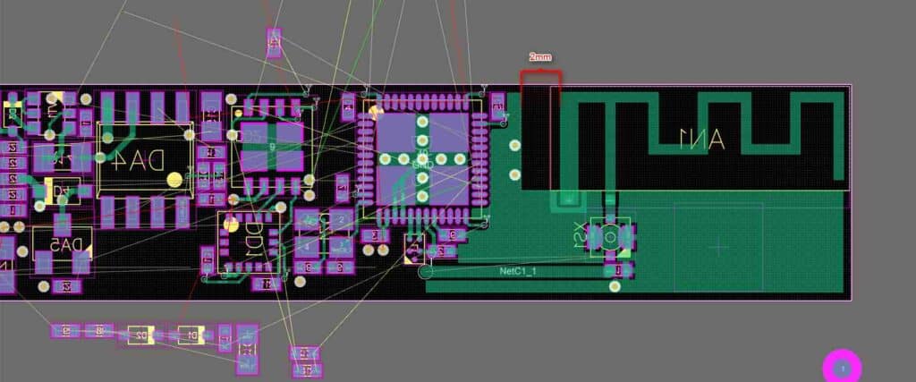
Overview of Two Layer PCB Design
Two layer PCB design is a commonly used technique in electronic circuit design. It involves the use of two layers of copper traces and vias to create a functional circuit. The top layer is used for the majority of the circuit components, while the bottom layer is used for ground and power planes.
One of the main advantages of two layer PCB design is its simplicity. It is easier and less expensive to manufacture than multi-layer PCBs. Additionally, it is easier to troubleshoot and repair since all the components are visible on the top layer.
Two layer PCBs are also more reliable than single layer PCBs since they offer better signal integrity and reduced electromagnetic interference. The use of ground and power planes on the bottom layer helps to reduce noise and improve signal quality.
However, there are some limitations to two layer PCB design. The routing of traces can be more challenging compared to multi-layer PCBs, and the number of components that can be used is limited due to the lack of space. In some cases, it may be necessary to use more layers for complex circuits.
In summary, two layer PCB design is a simple and reliable technique for electronic circuit design. It is ideal for simple to moderately complex circuits and offers good signal integrity and reduced electromagnetic interference. However, more complex circuits may require additional layers to accommodate the necessary components and routing.
Design Considerations for Two Layer PCBs
When designing a two layer PCB, there are several important considerations to keep in mind to ensure a successful and functional design. These considerations include trace routing, component placement, and the use of ground and power planes.
Trace Routing
Trace routing is a critical aspect of two layer PCB design. It is important to ensure that all traces are properly routed to avoid interference and signal loss. When routing traces, it is important to keep them as short and direct as possible. Avoid routing traces over other traces or components, as this can cause interference and crosstalk.
Component Placement
Component placement is another important consideration in two layer PCB design. It is important to place components in a way that minimizes signal interference and maximizes signal integrity. Keep components that generate noise, such as oscillators and clock generators, away from sensitive components such as analog circuits. Additionally, it is important to place components in a way that allows for efficient and neat routing of traces.
Ground and Power Planes
Ground and power planes are critical components of two layer PCB design. Ground planes provide a low impedance return path for signals, while power planes provide a stable voltage source for components. It is important to ensure that these planes are properly connected and routed to avoid interference and noise. Additionally, it is important to ensure that the ground plane is continuous and unbroken to provide a stable reference for all components.
In conclusion, designing a successful two layer PCB requires careful consideration of trace routing, component placement, and the use of ground and power planes. By keeping these considerations in mind, designers can create functional and reliable two layer PCBs.
Advantages of Two Layer PCB Design

Cost-effective
One of the biggest advantages of two layer PCB design is its cost-effectiveness. Two layer PCBs require fewer materials and less manufacturing time compared to multi-layer PCBs, which translates to lower production costs. Furthermore, the simplicity of two layer PCB design also makes it easier to repair and maintain, reducing costs associated with repairs and replacements.
Compact Size
Two layer PCBs are also known for their compact size. With only two layers of circuitry, these PCBs can be designed to be smaller and more lightweight than multi-layer PCBs. This makes them ideal for use in portable electronics and other devices where space is limited.
Ease of Manufacturing
Two layer PCBs are also easier to manufacture than multi-layer PCBs. The simpler design of two layer PCBs means that they can be produced faster and with fewer errors. This can help to reduce manufacturing time and costs, while also ensuring that the final product is of high quality.
Overall, the advantages of two layer PCB design make it a popular choice for many electronics manufacturers. With lower production costs, compact size, and ease of manufacturing, two layer PCBs are an excellent choice for a wide range of applications.
Disadvantages of Two Layer PCB Design
Limited Routing Space
One of the major disadvantages of two layer PCB design is the limited routing space available. With only two layers, it can be difficult to route all the necessary traces, especially in complex designs or designs with high component density. This can lead to signal integrity issues, as well as difficulty in fitting all the necessary components onto the board.
Difficult Signal Integrity
Another disadvantage of two layer PCB design is the potential for difficult signal integrity. With only two layers, there is less space for ground and power planes, which can lead to increased noise and interference. In addition, the routing of high-speed signals can be more difficult, as they require careful consideration of the routing and placement of components.
Overall, while two layer PCB design can be a cost-effective solution for simpler designs, it does come with some significant drawbacks. Designers must carefully consider the limitations of two layer design and weigh them against the benefits before deciding on the best approach for their particular project.
Tips for Designing Two Layer PCBs
Use Copper Pour
Copper pour is a technique that involves filling unused areas of the PCB with copper to create a ground plane. This technique can help to reduce the noise and interference in the circuit. It can also help to improve the thermal performance of the PCB.
When using copper pour, it is important to ensure that the copper does not come too close to the traces. This can cause issues with crosstalk, which can lead to signal integrity problems. It is also important to ensure that the copper pour is connected to the ground plane.
Minimize Crosstalk
Crosstalk is a phenomenon that occurs when two traces on a PCB interfere with each other. This can cause signal integrity problems and can lead to errors in the circuit. To minimize crosstalk, it is important to ensure that the traces are routed as far apart from each other as possible.
It is also important to ensure that the traces are properly terminated. This can be done by using series resistors or termination networks. These components help to reduce the reflections that can cause crosstalk.
Avoid Overcrowding
Overcrowding is a common problem in two layer PCBs. This occurs when there are too many components or traces on the board, and there is not enough space to route them properly. This can lead to signal integrity problems, and can also make the board difficult to manufacture.
To avoid overcrowding, it is important to plan the layout of the board carefully. This can be done by grouping components together, and by using multi-layer PCBs where necessary. It is also important to ensure that the traces are routed in a logical and efficient manner.
In conclusion, designing a two layer PCB can be a challenging task. However, by following these tips, you can ensure that your design is optimized for performance and manufacturability.
