Unknown Pin Altium Designer is a powerful software tool that is used for designing printed circuit boards (PCBs). It is a comprehensive platform that offers a range of features and capabilities, including schematic capture, PCB layout, and design verification. Altium Designer is widely used by engineers and designers in various industries, including aerospace, automotive, medical, and consumer electronics.
One of the most notable features of Unknown Pin Altium Designer is its intuitive user interface, which makes it easy for users to navigate and work with the software. The software also includes a range of design tools and libraries that can help users create complex designs quickly and accurately. Additionally, the software offers advanced features such as 3D visualization, signal integrity analysis, and design rule checking, which can help users ensure that their designs meet the highest standards of quality and performance.
Overall, Unknown Pin Altium Designer is a powerful and versatile software tool that can help engineers and designers create high-quality PCB designs quickly and efficiently. Whether you are working on a small project or a complex system, Altium Designer has the tools and capabilities you need to succeed.
Understanding Unknown Pin in Altium Designer
What is an Unknown Pin in Altium Designer?
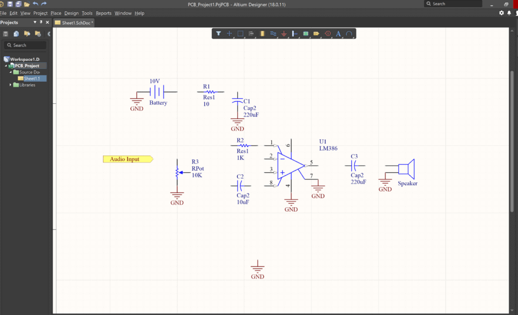
In Altium Designer, an unknown pin is a pin that has not been assigned a net name or a pin function. This means that the software does not know what the pin is connected to or what its purpose is. Unknown pins are usually represented by a question mark icon in the schematic editor.
Why Does Altium Designer Show Unknown Pins?
Altium Designer shows unknown pins for a few reasons. One reason is that a pin may not have been assigned a net name or a function yet. This can happen when a new component is added to the schematic or when a pin is added to an existing component. Another reason is that a pin may be connected to a net that has not been defined yet. In this case, the software cannot determine the net name for the pin.
To resolve unknown pins, the user must assign a net name or a pin function to the pin. This can be done by selecting the pin and assigning a net name or function in the Properties panel. Alternatively, the user can use the Place Net Alias command to assign a net name to a pin.
In conclusion, understanding unknown pins in Altium Designer is important for ensuring that the schematic is accurate and complete. By assigning net names and pin functions to unknown pins, the user can ensure that the design is properly connected and functional.
How to Resolve Unknown Pin in Altium Designer
Method 1: Assigning the Correct Footprint
If you encounter an unknown pin in Altium Designer, the first thing you can do is to check whether the correct footprint is assigned to the component. You can do this by following these steps:
- Open the PCB library editor.
- Find the component that has an unknown pin.
- Check whether the correct footprint is assigned to the component.
- If the correct footprint is not assigned, assign the correct footprint to the component.
Method 2: Updating the Library Component
If assigning the correct footprint doesn’t resolve the issue, you can try updating the library component. Here’s how you can do it:
- Open the PCB library editor.
- Find the component that has an unknown pin.
- Right-click on the component and select “Properties.”
- In the “Properties” dialog box, click on the “Models” tab.
- Check whether the correct model is assigned to the component.
- If the correct model is not assigned, update the library component with the correct model.
Method 3: Updating the Schematic Symbol
If the above methods don’t work, you can try updating the schematic symbol. Follow these steps:
- Open the schematic library editor.
- Find the schematic symbol that corresponds to the component with the unknown pin.
- Check whether the correct pin mapping is assigned to the schematic symbol.
- If the correct pin mapping is not assigned, update the schematic symbol with the correct pin mapping.
In conclusion, resolving unknown pins in Altium Designer can be done by assigning the correct footprint, updating the library component, or updating the schematic symbol. By following these methods, you can ensure that your design is error-free.
Common Mistakes to Avoid

Mistake 1: Using the Wrong Footprint
One of the most common mistakes that designers make is using the wrong footprint for a component. This can happen when a designer is in a rush or is not paying attention to the details. Using the wrong footprint can cause a variety of issues, including incorrect placement, soldering problems, and even electrical shorts.
To avoid this mistake, it is important to double-check the footprint before placing the component. Take the time to review the datasheet and ensure that the footprint matches the component’s specifications. Additionally, it is a good idea to create a library of commonly used footprints to ensure that you are using the correct one every time.
Mistake 2: Not Updating the Library Component
Another common mistake is not updating the library component when a new version of the component becomes available. This can cause issues when the component is used in future designs, as the outdated component may have different characteristics than the newer version.
To avoid this mistake, it is important to regularly check for updates to library components and update them as necessary. Additionally, it is a good idea to keep track of the changes made to library components to ensure that you are using the correct version in future designs.
Mistake 3: Not Updating the Schematic Symbol
Finally, another common mistake is not updating the schematic symbol when changes are made to the component. This can cause confusion when reviewing the schematic, as the symbol may not accurately represent the component.
To avoid this mistake, it is important to update the schematic symbol when changes are made to the component. Additionally, it is a good idea to review the schematic after making changes to ensure that the symbol accurately represents the component.
In summary, avoiding these common mistakes can help ensure that your designs are accurate and reliable. By double-checking footprints, updating library components, and updating schematic symbols, you can reduce the risk of errors and create high-quality designs.
