Table of Contents
ToggleA 3kW power amplifier driver circuit PCB layout is an essential component in the design of high-power audio systems. It is responsible for amplifying the low-level audio signals to high-level signals that can drive the power amplifier. The PCB layout is critical in ensuring that the amplifier operates efficiently and reliably.
The design of a 3kW power amplifier driver circuit PCB layout requires careful consideration of various factors, such as the type of amplifier topology, power supply, and heat dissipation. The layout must also be optimized to minimize noise and distortion, which can affect the quality of the audio output. A well-designed PCB layout can improve the overall performance of the amplifier and extend its lifespan.
In this article, we will explore the key considerations in designing a 3kW power amplifier driver circuit PCB layout. We will discuss the different amplifier topologies, the importance of power supply design, and the techniques for minimizing noise and distortion. By the end of this article, you will have a better understanding of the critical factors in designing a high-power amplifier driver circuit PCB layout.

PCB Layout Design
When designing a PCB layout for a 3kW power amplifier driver circuit, it is important to consider several factors such as power dissipation, component placement, and signal routing. In this section, we will discuss the various aspects of PCB layout design for a 3kW power amplifier driver circuit.
Power Amplifier Circuit Design
The power amplifier circuit design is the first step in the PCB layout design process. It involves selecting the appropriate amplifier topology and calculating the component values based on the desired output power and load impedance. The amplifier circuit design should be optimized for high efficiency and low distortion.
Schematic Design
Once the power amplifier circuit design is finalized, the next step is to create a schematic diagram. The schematic diagram should include all the necessary components and their interconnections. It should be clear and easy to understand, with proper labeling of all components.
Component Placement
Component placement is a critical aspect of PCB layout design. The placement of components affects the overall performance of the amplifier circuit. The components should be placed in a way that minimizes the length of signal paths, reduces crosstalk and noise, and maximizes heat dissipation.
Routing and Traces
The routing and traces of the PCB layout should be designed to minimize the resistance and inductance of the signal paths. The traces should be wide enough to handle the high current and should be routed in a way that minimizes interference with other components. The power and ground traces should be designed to handle the high current and should be kept as short as possible.
In summary, designing a PCB layout for a 3kW power amplifier driver circuit requires careful consideration of various factors such as power dissipation, component placement, and signal routing. By following the guidelines discussed in this section, you can create a PCB layout that is optimized for high efficiency and low distortion.
Power Amplifier Driver Circuit

Circuit Components
The power amplifier driver circuit is an essential part of any audio system. This circuit is responsible for amplifying the low-level audio signals to a higher level, which can be used to drive the power amplifier. The circuit comprises of various components, including resistors, capacitors, transistors, and diodes.
The resistors are used to limit the current flow, while capacitors are used to store and release electrical energy. Transistors are used as switches or amplifiers, and diodes are used to regulate the current flow.
Circuit Diagram
The circuit diagram of the power amplifier driver circuit is shown below. The circuit comprises of a pre-amplifier stage, a driver stage, and a power amplifier stage. The pre-amplifier stage amplifies the low-level audio signals, while the driver stage amplifies the signals to a higher level, which can be used to drive the power amplifier.
Amplifier Driver Circuit Design
The amplifier driver circuit design is crucial for achieving optimal performance. The circuit design should ensure that the amplifier driver can handle the required power and impedance of the load.
The amplifier driver circuit design should also consider the power supply requirements, input signal level, and output signal level. The circuit should be designed to minimize distortion and noise, and the components should be carefully selected to ensure optimal performance.
In conclusion, the power amplifier driver circuit is an essential part of any audio system. The circuit comprises of various components, including resistors, capacitors, transistors, and diodes. The circuit diagram comprises of a pre-amplifier stage, a driver stage, and a power amplifier stage. The amplifier driver circuit design should consider the power supply requirements, input signal level, and output signal level.
Testing and Troubleshooting

Testing Procedures
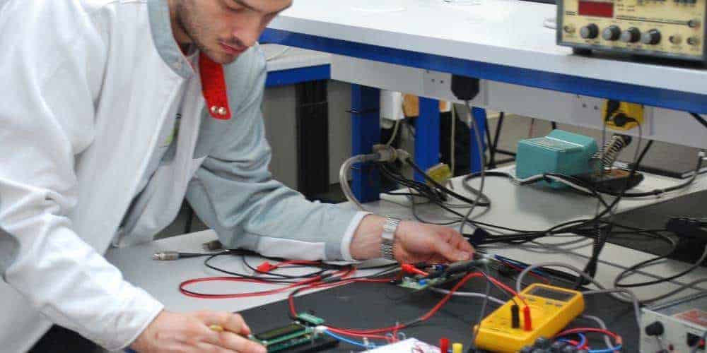
Once the 3kW power amplifier driver circuit PCB layout is complete, it’s important to test it thoroughly to ensure that it’s functioning properly. Here are the steps to follow when testing the circuit:
- Connect the power supply to the circuit and turn it on.
- Use a multimeter to measure the voltage at various points in the circuit to ensure that it’s within the expected range.
- Connect a signal generator to the input of the circuit and measure the output signal with an oscilloscope.
- Increase the input signal gradually and ensure that the output signal remains clean and undistorted.
- Measure the output power of the amplifier using a power meter and ensure that it’s within the expected range.
Troubleshooting Tips
If the circuit doesn’t function properly during testing, here are some troubleshooting tips to follow:
- Check all connections to ensure that they’re properly soldered and connected.
- Use a multimeter to check for continuity between various points in the circuit to ensure that there are no broken connections.
- Check that all components are properly installed and that there are no damaged components.
- Check that the power supply is providing the correct voltage to the circuit.
- Use an oscilloscope to check the input and output signals and look for any signs of distortion or other issues.
By following these testing procedures and troubleshooting tips, you can ensure that your 3kW power amplifier driver circuit PCB layout is functioning properly and is ready for use in your next project.
Conclusion
In conclusion, designing a 3kW power amplifier driver circuit PCB layout requires careful consideration of various factors such as power requirements, heat dissipation, and component selection.
Through this article, we have explored the key aspects of designing an efficient and reliable 3kW power amplifier driver circuit PCB layout. We have discussed the importance of selecting high-quality components that can handle the required power and minimize heat generation.
Additionally, we have emphasized the significance of proper heat dissipation techniques, such as using heat sinks and optimizing the layout for efficient airflow.
Finally, we have touched on the importance of following industry-standard design practices and guidelines to ensure the longevity and reliability of the circuit.
Overall, designing a 3kW power amplifier driver circuit PCB layout requires a thorough understanding of the underlying principles and careful attention to detail. By following the guidelines outlined in this article, you can create a robust and efficient design that meets your power requirements and delivers reliable performance.

