Power supply circuits are an essential component of any electronic device, providing the necessary voltage and current to power the circuitry. The printed circuit board (PCB) layout of a power supply circuit is a critical aspect that can significantly affect the performance and reliability of the circuit. Proper PCB layout design can help minimize noise, reduce electromagnetic interference, and ensure efficient power transfer.
When designing a power supply circuit PCB layout, it is crucial to consider various factors such as component placement, trace routing, and grounding. The placement of components on the PCB can impact the circuit’s performance, and it is essential to ensure that components are placed optimally to minimize noise and interference. Trace routing is another critical aspect of PCB layout design that can affect the circuit’s performance. Proper trace routing can help minimize voltage drops and ensure efficient power transfer. Grounding is also crucial in power supply circuits, and proper grounding techniques can help reduce noise and improve the circuit’s performance.

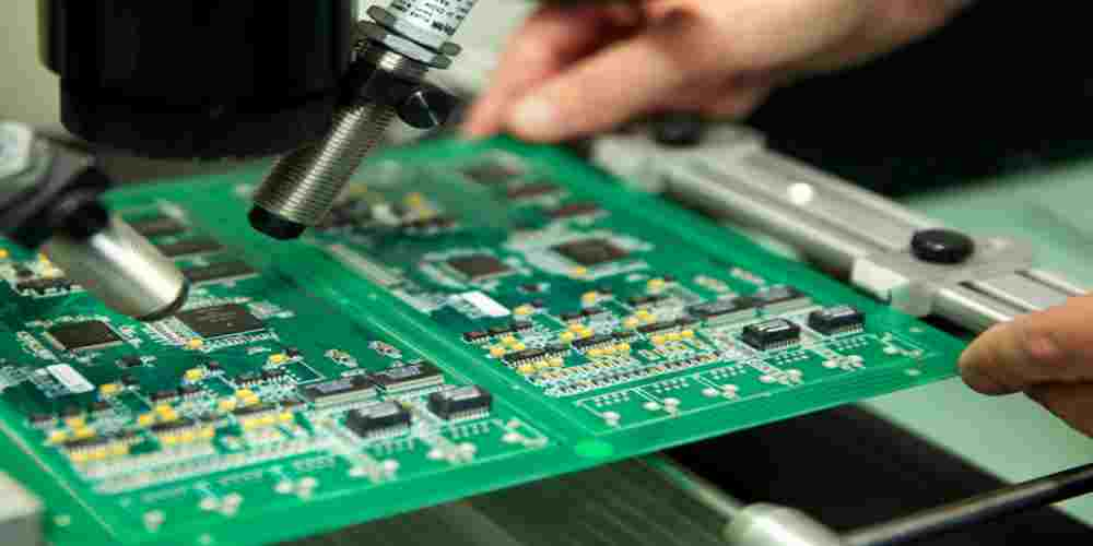
Basics of Power Supply Circuit PCB Layout
When designing a power supply circuit, the PCB layout is crucial for ensuring proper functionality and reliability. Here are some basics to consider when laying out your power supply circuit PCB.
Components Placement
The placement of components on the PCB can greatly affect the performance of the power supply circuit. It is important to place components in a way that minimizes noise and interference. Here are some tips for component placement:
- Keep components that generate noise, such as switching regulators, away from sensitive components like analog circuits.
- Place decoupling capacitors as close as possible to the power pins of the ICs they are decoupling.
- Place components in a logical and organized manner, making it easier to troubleshoot and repair the circuit if necessary.
Trace Routing and Width
Trace routing and width are important considerations for power supply circuit PCB layout. Here are some tips for trace routing and width:
- Keep traces as short as possible to minimize resistance and inductance.
- Use wider traces for high current paths to reduce voltage drop.
- Avoid sharp corners in traces, as they can cause reflections and signal degradation.
- Use ground planes to reduce noise and improve signal integrity.
Ground and Power Planes
Ground and power planes are essential for power supply circuit PCB layout. Here are some tips for ground and power planes:
- Use a solid ground plane to provide a low impedance return path for signals and reduce noise.
- Use a power plane to distribute power to components and reduce voltage drop.
- Keep the ground and power planes as close together as possible to reduce noise.
- Use vias to connect the ground and power planes on different layers.
By following these basics of power supply circuit PCB layout, you can ensure that your power supply circuit is reliable and performs as intended.
Design Considerations for Power Supply Circuit PCB Layout

When designing a power supply circuit PCB layout, there are several important factors to consider. This section will cover some of the key design considerations that should be taken into account.
EMI/EMC Considerations
Electromagnetic interference (EMI) and electromagnetic compatibility (EMC) are important considerations when designing a power supply circuit PCB layout. EMI can cause interference with other electronic devices, while EMC ensures that the power supply circuit is not affected by external interference.
To minimize EMI, it is important to keep the traces short and use proper grounding techniques. Shielding can also be used to reduce EMI. To ensure EMC, it is important to use proper filtering and decoupling techniques.
Thermal Considerations
Thermal considerations are also important when designing a power supply circuit PCB layout. Heat can be generated by the power supply circuit, which can affect the performance and reliability of the circuit.
To minimize heat, it is important to use proper thermal management techniques, such as heat sinks and thermal vias. The placement of components can also affect the thermal performance of the circuit.
Safety Considerations
Safety is a critical consideration when designing a power supply circuit PCB layout. The power supply circuit must be designed to ensure that it is safe to use and does not pose a risk of electric shock or other hazards.
To ensure safety, it is important to use proper insulation and grounding techniques. The power supply circuit should also be designed to comply with relevant safety standards and regulations.
Overall, designing a power supply circuit PCB layout requires careful consideration of several important factors, including EMI/EMC, thermal, and safety considerations. By taking these factors into account, it is possible to design a safe, reliable, and high-performance power supply circuit.
Advanced Techniques for Power Supply Circuit PCB Layout
Multi-Layer PCB Design
Designing a multi-layer PCB is an advanced technique that can improve the performance of a power supply circuit. Multi-layer PCBs provide additional space for routing power and ground planes, reducing noise and improving signal integrity.
When designing a multi-layer PCB, it is essential to consider the number of layers required, the placement of the power and ground planes, and the routing of signals. A good practice is to use a minimum of four layers, with the outer layers dedicated to routing signals and the inner layers used for power and ground planes.
Via Stitching
Via stitching is a technique used to connect multiple ground planes together, reducing the noise generated by the power supply circuit. Via stitching involves placing vias around the perimeter of the ground plane, creating a conductive path for noise to be absorbed.
When using via stitching, it is essential to place the vias as close together as possible and to use a sufficient number of vias to ensure a low impedance path for noise to be absorbed.
Component Density Optimization
Component density optimization is an essential technique for designing a compact power supply circuit PCB. By optimizing the placement of components, it is possible to reduce the size of the PCB while maintaining performance.
When optimizing component density, it is essential to consider the placement of high-frequency components, such as capacitors and inductors, and the routing of power and ground traces. A good practice is to place high-frequency components as close as possible to the IC and to use a ground plane to reduce noise.
In conclusion, designing a power supply circuit PCB requires careful consideration of advanced techniques such as multi-layer PCB design, via stitching, and component density optimization. By implementing these techniques, it is possible to improve the performance of a power supply circuit while reducing the size of the PCB.
