Printed circuit boards are available in different layers. Multilayer PCBs have a huge impact on today’s electronics. A 6 layer PCB is a good example of a multilayer PCB. This board has contributed to the development of some electronic devices. This article discusses everything you need to know about a 6 layer PCB.
What is a 6 Layer PCB Stackup?
A 6 layer PCB consists of six different layers of conductive material. It is a circuit board that features a 4 layer PCB and two signal layers. PCB manufacturers place these signal layers between the planes. A 6 layer PCB stackup has four routing layers and two internal planes. The four routing layers are both external and internal layers.
The design of a 6 layer PCB helps to boost EMI and also provides better routing for signals. A 6 layer PCB has two surface layers and two buried layers. The buried layers direct fast speed signals while the surface layers direct low-speed signals. In a 6 layer PCB stackup, the arrangement of the insulating layers and copper layers matters.
For a 6 layer PCB stackup, the general layers are the power plane, ground plane, and inner signal layers. The arrangement of this stackup ensures the circuit board has the best signal. It is very important to create the right configuration of layers. This helps to improve the circuitry’s performance.
What Makes up a 6 Layer PCB Stackup?
A 6 layer PCB stackup comprises different layers. The ground plane, power plane, and signal layers make up a 6 layer PCB stackup. Each of these layers has its functions. However, it is important to understand how these layers play a significant role in the functionality of this stackup.
Ground plane
The ground plane functions as a return path for current from various components on the circuit. It is a layer of copper foil that connects to the ground point of the circuit. This separate layer is so large that it covers the whole board. The ground plane allows the PCB manufacturer to ground components easily.
Power plane
This is a plane of copper that connects to a power supply. The power plane provides a supply of voltage to the circuit board. This layer is often seen in multilayer stackups since these stackups use an even number of layers. A power plane reduces the operating temperature of a board as it can handle more current.
Signal layers
These layers include the bottom layer, top layer, and inner layer. All these layers have electrical connections.
- Bottom signal layer: This layer is primarily for soldering and wiring. For a multilayer board, manufacturers can place components.
- Top signal layer: It is also referred to as thecomponent layer. This layer is used to arrange copper or wires.
- Inner signal layer: This layer is connected to power and ground planes. It has electrical connections and consists of an entire piece of the copper film. The inner signal layer can only be seen in multilayer boards.
Types of Configuration on a 6 Layer PCB Stackup
For a 6 layer PCB stackup, several arrangements or configurations are put in place. The type configuration on this stackup depends on the requirements of the intended application. If signal control is an important factor, the number of signal layers has to increase. However, if high-speed circuitry is important you will opt for configurations with the best shielding.
First Type
- Top signal
- Inner signal
- Ground plane
- Power plane
- Inner signal
- Bottom signal
This first type of configuration doesn’t protect signal layers properly. It was one of the first configurations used in past years. PCB manufacturers need to reduce the bottom layer and the top layer to ensure signal mutual interference. When signal performance became important, manufacturers began to abandon this configuration type.
Second Type
- Top signal
- Ground plane
- Inner signal
- Inner signal
- Power plane
- Bottom signal
This second type of configuration is very common. It provides proper protection for the inner signal layers. This configuration is very ideal for PCBs operating in high signals. You can use a thicker dielectric material to increase the distance between the inner signal layers. This will help to enhance the stackup. The limitation of this configuration type is that there is a reduction in planner capacitance. This is caused by the separation of the ground and power planes.
Third Type
- Top signal
- Ground plane
- Inner signal
- Power plane
- Ground plane
- Bottom signal
In this third type of configuration, each signal layer is placed adjacent to a ground plane. This helps to ensure the best return path. When the ground and power plane are close to each other, there is planner capacitance.
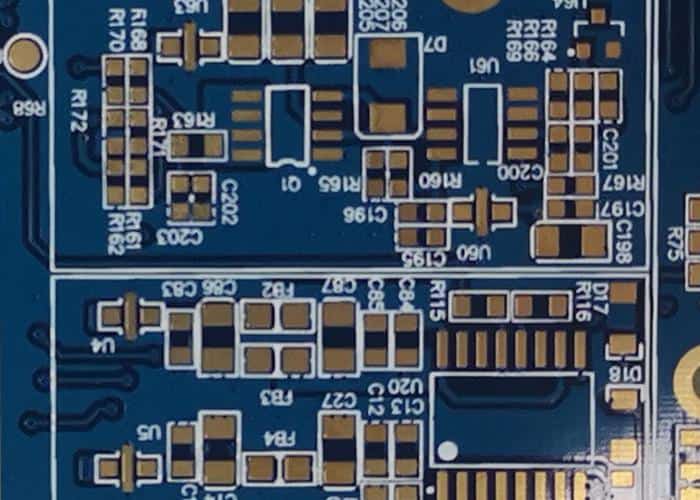
6 Layer PCB Fabrication
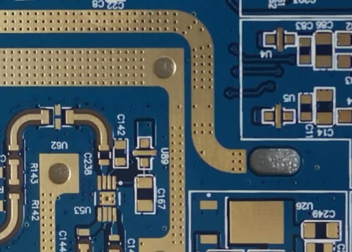
The fabrication of a 6 layer PCB requires serious attention. During the fabrication of this PCB, the manufacturer presses the board from the core and coats it with copper coil. A core board is a 4 layer PCB while two core boards are 6 layer boards. Below are 6 layer PCB fabrication and design skills.
Edit the schematic diagram
The 6 layer PCB can feature two layers of the ground plane in the circuit board. This means that the manufacturer can separate the digital and analog grounds. Involve the signal’s minimum return path in EMI. Ensure you check for any errors after creating the schematic diagram.
Create a new PCB file
After the manufacturer has created a new PCB file, the schematic netlist can be imported into that file. The manufacturer then sets the layer structure and adds layers. The next thing is to add the power and ground layers. During a 6 layer PCB fabrication, you must couple the main ground layer and the power layer. This should be at a distance of 5 ml.
Layout
Layout is very important in the fabrication of a 6 layer PCB stackup. The primary principle of layout is to ensure good partition. Moreso, the partition of digital and analog devices can help to minimize interference. Digital signals generate large interference and a strong anti-interference.
You need to check out the components layout with various operating voltages. Ensure that devices having large voltage differences are far apart. In principle, the best configuration type features 3 power layers and 3 signal layers. The ground plane is the second and fifth layers. The third and fourth layers are power and inner signal layers.
Ground plane production
In a 6 layer PCB fabrication, there are two layers of ground. They are DGND and AGND. The DGND is placed on the fourth layer while the AGND is placed on the second layer. The manufacturer uses wires to lead out the pins of the ground and top components. Then you use the via hole to connect the pins to the corresponding network. Ensure you use a few pads during the connection process. This is because the pads will increase interference.
Power plane production
You need to divide the power layer. This is because the 6 layer PCB will not feature one working voltage value. Follow these procedures for segmentation during a 6 layer PCB fabrication;
- Figure out a voltage network
- Change to the inner power layer
- Draw a closed graph using a line
- Use wires to lead out the pins of the ground and top layer
- Create connection to the inner power layer via the pad
- Design the next power network
Routing
Ensure the ground layer and power layer are made well. After this, route the signal lines. Routing during a 6 layer PCB fabrication requires serious attention. The manufacturer should ensure that the vital high-speed signal line goes to the inner signal layer. The signal can also move on its ground layer.
For instance, if analog signals are mostly on the top layer, the second layer should be set to AGND. Furthermore, you need to adjust the component layout appropriately to enhance wiring. The routing method for the inner signal layer is wire-pad –inner electric layer.
DRC Inspection
This is an important step for a 6 layer PCB fabrication. DRC simply means design rule check. After the manufacturer has drawn the board, the inspection must take place. Carrying out a DRC helps to enhance the fabrication yields of a 6 layer PCB.
Instructions for a 6 Layer PCB Manufacturer
The manufacturing of a 6 layer PCB requires extreme care and attention. A 6 layer PCB manufacturer needs to be aware of certain things during manufacturing. Below are certain instructions that should be carried out during manufacturing;
- Ensure you carry out differential wiring, and set wiring groups for important signals
- Arrange cables for BGA packaged devices. After this, lead out the external two layers of pins and arrange the cables.
- The data line should be a cluster and isolate the clock line from the data line.
- Ensure the nodes of the circuit board are accessible to the wires. This will make the PCB easy to use.
- To make the metal core circuit board accessible, give some space between the electrical components. Place components of the same category on the circuit board.
- To enhance the performance of an electrical component, the bypass capacitors should be placed in the components.
- Lead the wire out during wiring to prevent the wiring from becoming dense.
- Place decoupling capacitors in a parallel with the signal vias.
How to Choose the Best 6 Layer PCB Manufacturer
Choosing the best 6 layer PCB manufacturer is very important for your PCB design. A good manufacturer must be very efficient and reliable. Below are factors to consider;
Experience
You will need to know how long the manufacturer has been doing this. Experience determines the quality of the PCB design. Choose a reliable manufacturer that has long-standing experience in 6 layer PCB fabrication.
Certifications
Choose a PCB manufacturer with the right certifications. The best PCB manufacturer produces a board that meets certain standards of the PCB industry.
Good turnaround time
The turnaround time refers to how long it takes to complete an order. You want a manufacturer that delivers quality boards within a specific turnaround time. Your manufacturer should maintain a good turnaround time while delivering quality.
Customer support
You definitely want a PCB manufacturer that ensures your needs are met. Choose a manufacturer that is responsive to the needs and complaints of its clients.
Applications of a 6 Layer PCB Stackup
A 6 layer PCB is widely used in various industries. This is as a result of its functionality and benefits. 6 layer PCBs are the best way to achieve improved functionality. Due to this, they have become popular in many applications.
Consumer electronics
A 6 layer PCB stackup is ideal for use in the production of most consumer electronics. Consumer electronics include microwaves, smartphones, smartwatches, remotes, radios, and more. The majority of today’s consumer electronics feature 6 layer PCBs.
Telecommunications
Some telecommunication devices feature a 6 layer PCB because of its unique benefits. GPS, satellite, and signal transmission use this multilayer PCB.
Medical devices
The manufacturing of some medical devices requires the use of 6 layer PCBs. Scan equipment, X-ray machines, and heart monitors among others feature these boards.
Automotive
Some parts of a vehicle feature 6 layer PCBs. For example, engine sensors and headlight switches feature this type of PCB. The use of a 6 layer PCB stackup is important in automotive design. Several automobile manufacturers utilize this PCB because of its functionality.
Industrial
A 6 layer PCB stackup is an ideal choice for the production of some industrial devices. This is because of the vigorous use of most industrial devices. A 6 layer PCB is known for its durability and enhanced functionality.
Conclusion
By now, you should have gained much knowledge about 6-layer PCB design. The way the board layer stackup is created plays a vital role in how successful the 6-layer PCB design will be. Fortunately, the PCB design tools of today allow the addition and deletion of layers from the design. By doing so, you will be able to choose the best layer configuration for your needs. The best part here is choosing a design system for your PCB that gives you the best power and flexibility, which allows the easy creation of the 6-layer stackup type for your design.
