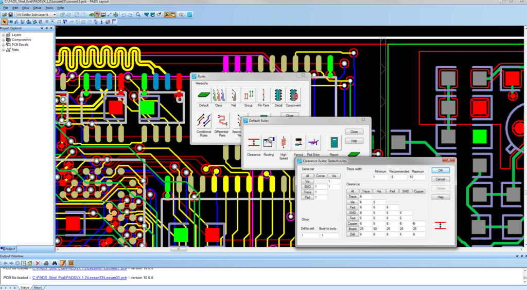
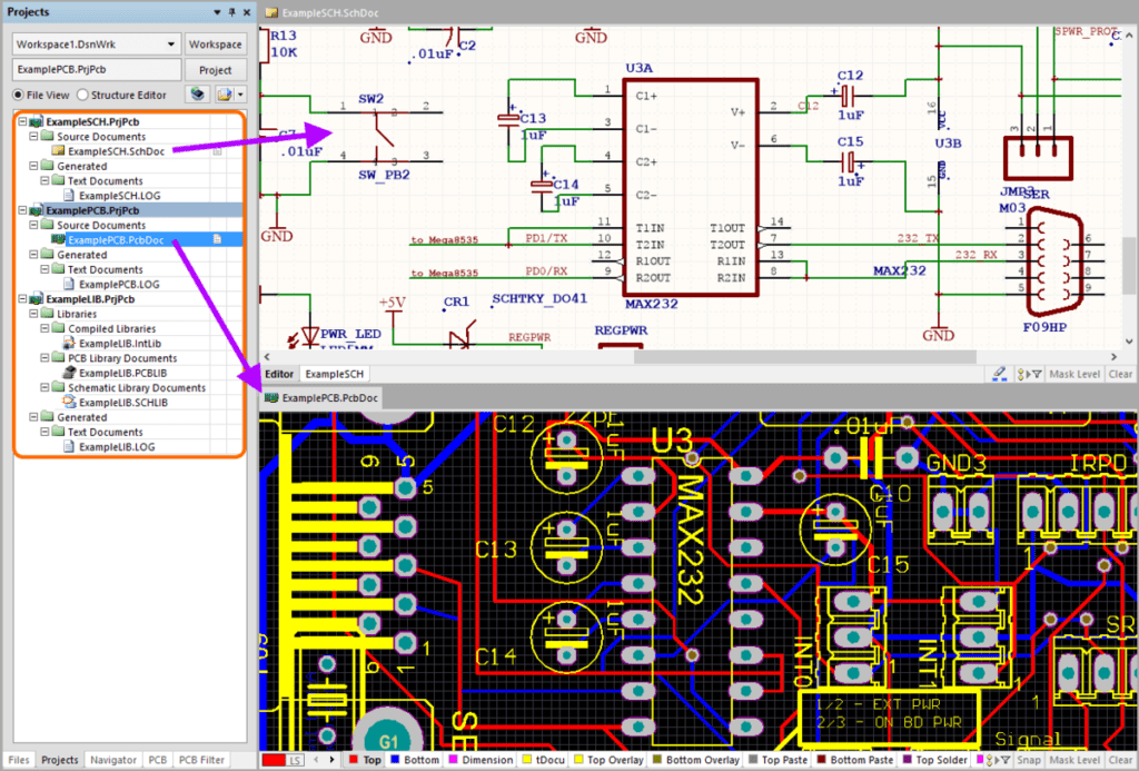
Altium Designer is a popular software tool used by electronic engineers for designing printed circuit boards (PCBs). One of the key features of Altium Designer is its cross-probing capabilities. Cross-probing is the ability to highlight a component or net on the schematic and have it highlighted on the PCB layout, and vice versa.
The cross-probing feature in Altium Designer is a powerful tool that helps engineers to easily navigate between the schematic and layout views of their design. With cross-probing, engineers can quickly identify and resolve any discrepancies between the schematic and layout, ensuring that the final PCB design is accurate and error-free. Additionally, cross-probing can help to speed up the design process by allowing engineers to quickly locate and modify components or nets on either the schematic or layout view.
Overall, the cross-probing feature in Altium Designer is an essential tool for any electronic engineer looking to design high-quality, error-free PCBs. By allowing engineers to easily navigate between the schematic and layout views of their design, cross-probing helps to streamline the design process and ensure that the final product is accurate and meets all design specifications.
What is Altium Designer?
Altium Designer is a powerful electronic design automation (EDA) software that is used to design printed circuit boards (PCBs). It is an all-in-one solution that provides a comprehensive set of tools for schematic capture, PCB layout, and design verification.
Altium Designer is widely used by engineers, designers, and other professionals in the electronics industry. It is known for its intuitive user interface, powerful design capabilities, and advanced features that help users to create high-quality designs quickly and efficiently.
Some of the key features of Altium Designer include:
-
Schematic capture: Altium Designer provides a powerful schematic capture tool that allows users to create and edit electronic schematics quickly and easily. The tool includes a comprehensive library of components that can be easily added to schematics.
-
PCB layout: Altium Designer provides a powerful PCB layout tool that allows users to create and edit PCB layouts quickly and easily. The tool includes a comprehensive library of components that can be easily added to PCB layouts.
-
Design verification: Altium Designer includes a range of design verification tools that help users to ensure that their designs are error-free and meet their specifications. These tools include design rule checking, netlist comparison, and signal integrity analysis.
Overall, Altium Designer is a powerful and versatile EDA software that provides a comprehensive set of tools for designing high-quality PCBs. Whether you are a professional engineer or a hobbyist, Altium Designer can help you to create designs quickly and efficiently.
What is Cross Probe?
Cross Probe is a powerful feature in Altium Designer that allows users to quickly and easily navigate between schematic and PCB design files. It enables users to select an object in one file and have the corresponding object highlighted in the other file, making it easier to locate and modify components and connections.
This feature is particularly useful for complex designs, where it can be difficult to keep track of all the connections and components. With Cross Probe, users can quickly identify and resolve any issues, reducing the likelihood of errors and saving time in the design process.
To use Cross Probe, simply select an object in either the schematic or PCB design file and then right-click and choose the Cross Probe option. The corresponding object will be highlighted in the other file, making it easy to see exactly where it is located and how it is connected.
Overall, Cross Probe is an essential tool for anyone working with complex designs in Altium Designer. It can help to streamline the design process, reduce errors, and improve overall efficiency.
How to Use Cross Probe in Altium Designer

Setting up Cross Probe
Before using Cross Probe in Altium Designer, you need to set it up. To do this, follow these simple steps:
- Open your schematic and PCB documents.
- Go to the Preferences menu and select Cross Probe.
- In the Cross Probe dialog box, select the settings you want to use. You can choose to show the cross-probe highlight, set the highlight color, and choose whether to show the highlight on the schematic or PCB.
- Click OK to save your settings.
Using Cross Probe to Navigate Between Schematic and PCB
Once you have set up Cross Probe, you can use it to navigate between your schematic and PCB documents. Here’s how:
- Select the component or net you want to cross-probe in either the schematic or PCB document.
- Right-click on the component or net and select Cross Probe from the context menu.
- The other document will now be opened, and the cross-probed component or net will be highlighted.
Customizing Cross Probe Settings
In addition to the basic settings, you can also customize Cross Probe in Altium Designer to suit your specific needs. Here are a few examples of what you can do:
- Change the highlight color: If you find the default highlight color difficult to see, you can change it to something more visible.
- Show the highlight on both documents: If you prefer, you can choose to show the cross-probe highlight on both the schematic and PCB documents.
- Use hotkeys: You can assign hotkeys to the Cross Probe function to make it even easier to use.
To customize Cross Probe, go to the Preferences menu, select Cross Probe, and choose the settings you want to change.
That’s it! With these simple steps, you can use Cross Probe in Altium Designer to navigate between your schematic and PCB documents quickly and efficiently.
Benefits of Using Cross Probe in Altium Designer
Efficient Design Process
Cross Probe is a powerful feature in Altium Designer that allows designers to quickly navigate between schematic and PCB views. By simply clicking on a component in the schematic view, users can instantly highlight the corresponding component in the PCB view, and vice versa. This makes it easy to identify and correct any discrepancies between the two views, saving valuable time and streamlining the design process.
Improved Accuracy and Quality Control
Cross Probe also helps to ensure accuracy and quality control in the design process. By providing a visual link between schematic and PCB views, designers can easily verify that all components are correctly placed and connected. This reduces the risk of errors and improves the overall quality of the design.
Saves Time and Reduces Errors
One of the biggest benefits of using Cross Probe in Altium Designer is the time savings it provides. By eliminating the need to manually search for components and connections between schematic and PCB views, designers can work more efficiently and complete their designs faster. This also reduces the risk of errors, as designers are less likely to miss important connections or components.
Overall, Cross Probe is a valuable feature in Altium Designer that can greatly improve the design process. By enabling efficient navigation between schematic and PCB views, improving accuracy and quality control, and saving time and reducing errors, Cross Probe is a must-have tool for any Altium Designer user.
Conclusion
In conclusion, Altium Designer’s cross-probing feature is a powerful tool that can save time and improve accuracy in PCB design. By allowing users to quickly and easily navigate between schematic and PCB views, cross-probing ensures that design changes are accurately reflected in both views.
Some of the key benefits of cross-probing in Altium Designer include:
- Efficient navigation between schematic and PCB views
- Improved accuracy and consistency in design changes
- Reduced risk of errors and design inconsistencies
Overall, cross-probing is an essential feature for any PCB designer using Altium Designer. By taking advantage of this powerful tool, designers can streamline their workflow and improve the quality of their designs.
