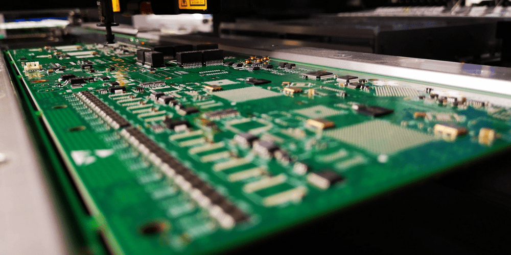
High-Density Interconnect Printed Circuit Board (HDI PCB) refers to the type of circuit board that offers improved properties than the conventional boards do. With the introduction of the HDI technology into consumer electronics optimization, these devices now have improved spacing.
One of the advantages to using a HDI PCB is the higher wiring density. Besides, one can leverage the circuit board to incorporate or add more components into the Printed Circuit Board (PCB).
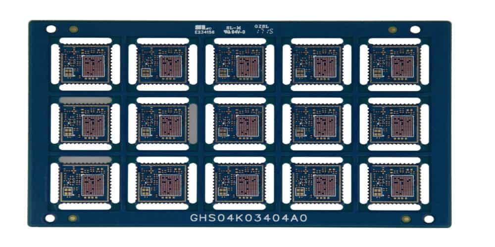
Today, there are hundreds of HDI PCB manufacturers offering this type of circuit board design in different parts of the world. We have curated a list of the top eight (8) HDI PCB manufacturers, as well as pointed out the reasons why they are different from the other manufacturers.
1. Rayming PCB & Assembly

Also known as Rayming Technology or RayPCB, this is one of the HDI PCB manufacturers you can trust. Located in Shenzhen, China, we offer a wide range of HDI PCB services.
One core area we focus on is the stackup, which plays an important role in how the circuit board is optimized to function. For emphasis, RayPCB uses the following HDI PCB stackup or structure:
1+N+1, 2+N+2, 3+N+3, 4+N+4 and any layer in R&D.
Here is a breakdown of the RayPCB HDI PCB stackup:
- 1+N+1: this means that the Printed Circuit Board (PCB) we fabricate will have only one build-up of the High-Density Interconnect (HDI) layers.
- 2+2+2: just like the above, this refers to the number of build-ups of the HDI layers the PCB has. In this case, it is two (2).
- 3+N+3: this type of HDI PCB has three build-ups of the HDI layers.
- Any Layer HDI PCB: this refers to the HDI PCB that has all the layers of the Printed Circuit Board (PCB0 as High-Density Interconnect (HDI) layers. We use this HDI PCB stackup because it allows for the flexible interconnection of the conductors on any layer of the PCB. The interconnection is made with the any layer via – the copper-filled or populated stacked microvia structures.
RayPCB’s HDI PCB Capabilities
The following are some of the reasons why HDI PCB consumers prefer having RayPCB to handle the fabrication:
- Multiple HDI PCB Design Technologies: there are different design processes used when fabricating the HDI PCB. RayPCB maximizes as many of these as possible. For example, we are experts at using the following HDI PCB technologies: tiny circuit, microvia manufacturing, and the through-hole metallization processes.
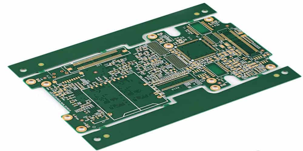
- Specialized Fabrication Typologies: different types of HDI PCBs exist. RayPCB helps you to fabricate these circuit boards, as per the target applications. The following are some of the HDI PCB types we fabricate: Multilayer HDI PCB, Flexible HDI PCB, Rigid-Flexible HDI PCB, and Rigid HDI PCB.
- Several Material Options: we also use different kinds of materials when manufacturing the HDI PCB. The following are some of the supported materials: First Generation Microvias, High-Temperature FR4, and Halogen-free materials.
2. PCBcart
PCBcart is a full-service PCB fabrication and assembly service provider in China. The company believes that PCB consumers, including those ordering for the HDI PCB, should get value for their investments.
That informs the reason behind the manufacturer’s dedication to making in-house checks, raising the standards of the HDI PCB, while offering an excellent customer service.
HDI PCB Capabilities
We were able to verify that PCBcart specializes in offering the following HDI PCB services:
- Competitive Pricing: besides the improved design of the HDI PCB, the manufacturer also pays attention to the market yearnings. PCBcart understands that not all consumers may afford to make bulk purchases of the circuit board, hence, the decision to wave the Minimum Order Quantity (MOQ). Interestingly, you get to enjoy competitive pricing no matter how many HDI PCBs you are ordering for.
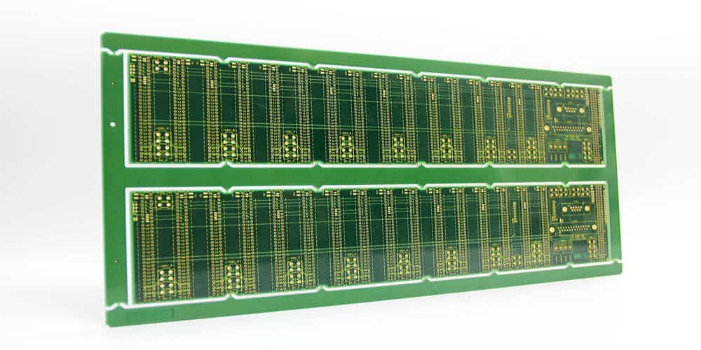
- Multi-Layer Capabilities: PCBcart promises to fabricate different layers of the HDI PCB, up to 24 layers. These fabrications are done in addition to offering the HDI PCB in different structures.
- HDI PCB Fabrication Process: the manufacturer deploys different HDI PCB techniques. These include the popular via in pad, flex-rigid combination and the buried capacitor. The buried capacitor technique is exclusively used for the prototypes of HDI PCBs measuring less than 1 meter square.
- Materials Used: PCBcart uses different kinds of materials, such as the FR4 and Rogers lamination combination, FR4 standard Tg 140˚C, and the FR4 High Tg 170˚C.
- HDI PCB Surface Finishes: the following are examples of the surface finishes used by PCBcart: Organic Solderability Preservatives (OSP), Immersion Silver, Lead Free HASL, Immersion Tin, Hot Air Solder Leveling (HASL), and the Electroless Nickel/Immersion Gold (ENIG). A majority of these surface finishes are RoHS-compliant.
- Production Capabilities: PCBcart has a variety of HDI PCB production capabilities. For example, the company has a flexible build time of 2 days and 5 weeks maximum. It also engages in HDI PCB prototyping, mass production and small-middle batch production of the HDI PCBs using the blind vias, blind/buried stacked vias and the blind/buried staggered vias micro vias typologies.
3. PCBMay
PCBMay is a professional HDI PCB manufacturing company. The company has been offering this service in China for over 12 years. They are the go-to for different kinds of HDI PCBs, with an emphasis on quick-turn service and prototyping of the circuit boards.
HDI PCB Capabilities
Below are some of the HDI PCB capabilities of PCBMay:
Multi-Step HDI PCBs
This refers to the different build-ups or stackups of the High-Density Interconnect PCB (HDI PCB). PCBMay specializes in manufacturing HDI PCBs with the following structures:
- 1 Step HDI PCB: this type of HDI PCB contains only one build-up of the High-Density Interconnected (HDI) layers.
- 2 Step HDI PCB: it uses two HDI layers. In addition, the 2 Step HDI PCB allows for the micro vias to either be stacked or staggered across the layers.
- 3 Step HDI PCB: this refers to the two or more build-up layers that have a rigid core. It also allows through vias buried in the core and from surface to surface.
- 4 Step HDI PCB: this uses laser drills to create laser micro vias. The drills potentially generate up to 20 microns in diameter. It is pertinent to mention that the tiny and clean holes can be created via the drills cutting through both glass and metal.
- 5 Step HDI PCB: this is a 12-layer HDI with an emphasis on using the Laser Direct Imaging (LDI) technology.
- 6 Step HDI PCB: it is a 14-layer HDI, which requires up to 6 laminations.
4. MADPCB
MADPCB offers HDI PCB fabrication services from the headquarters in Shenzhen, China. The manufacturer helps thousands of HDI PCB consumers from different parts of the world optimize the boards as per the applications.
HDI PCB Production Options
Whether you are looking to fabricate the boards, have them in mass production or simply need a few prototypes – you can rely on MADPCB. The company specializes in mass production and prototyping of the High-Density Interconnect (HDI) PCB.
HDI PCB Construction Capabilities
For the construction of the HDI PCBs, MADPCB supports from HDI PCB types I to VI. The manufacturer also supports the 1+N+1, i+N+I (i>=2), and the Any Layer HDI (ELIC).
MADPCB Offers Professional HDI PCB Design
The company specializes in offering different kinds of HDI PCB design techniques. The following are the common technologies used:
- Laser Direct Imaging (LDI) Technology: this HDI PCB technology helps to maintain an excellent defect detection, make fine traces and spacings on the circuit board.
- Laser Drilling Technology: this type of PCB drilling technology is better than the mechanical drilling process, in the sense that the drilling process doesn’t get into contact with the PCB material.
5. Photronix Limited
This HDI PCB manufacturer is based in West Sussex, in the United Kingdom. Photronix Limited specializes in the fabrication of multilayer HDI PCBs, up to 22 layers.
The following is a breakdown of the company’s capabilities:
- Global HDI PCB Services: without being limited to the UK market, Photronix Limited ships worldwide. The company is able to do this because of the ISO 9001 accreditation.
- High-Quality HDI PCBs: Photronix Limited also ships the best HDI PCBs, with an emphasis on the consumer’s requirements.
- Materials: the manufacturer uses the following HDI PCB materials: Rogers, FR4 standard materials, and Halogen-free FR4 materials. The company also uses the FR4 high-performance materials.
- Microvias Optimization: Photronix Limited optimizes the microvias to be placed on the surface pads, as well as to only penetrate the selected layers.
- HDI PCB Surface Finishes: the following surface finishes are available – Gold Fingers, OSP, Electrolytic Gold, Immersion Tin, ENIG and Immersion Silver.
- Dimensions: the maximum dimension of the HDI PCB is 610mm by 450mm, although this often depends on the laser drilling machine.
- Thickness: the minimum thickness is 0.40mm, while the maximum thickness is 3.0mm.
6. Hemeixin Electronics Co., Limited
Hemeixin is an “elite provider of custom PCB fabrication services.” The company specializes in providing quick-turn production of the HDI PCB, as well as making quick-turning of the Printed Circuit Board Assembly (PCBA).
Here is a laydown of the different HDI PCB services the company offers:
HDI Micro Vias PCB
This type of HDI PCB encompasses the buried via and the blind via. The HDI Micro Vias PCB generally comes in handy when making HDI circuit boards that need interconnection of the layers, even amidst limited spaces.
HDI Flexible PCB
As the name signifies, this is the flexible version of the HDI PCB. Hemeixin manufacturers between 3 and 16 layers of the HDI Flex PCB. The company also uses the copper via fill, incorporates the blind via and buried via in a sequential build technology, as well as maximizes the panel density via the 45.7 cm x 61 cm panel size.
HDI PCB Stackup
Out of the three (3) common HDI PCB stackups, Hemeixin prefers to work with the lamination buildup, because of the compatibility with the HDI PCBs that have high pin-count Ball Grid Arrays (BGAs). The lamination buildup also works best with the other fine-pitch packages.
7. Kingford Technology Co., Limited
Known as Kingford for short, this HDI PCB manufacturer offers all-around HDI PCB fabrication service. The company helps you source for the HDI PCB components, offers fast turnaround and ensures that the circuit boards meet the highest standards.
For context, the company has the following certifications, confirming the commitment to improving the quality assurances of the HDI PCBs:
- UL
- ISO 9001
- IATF 16949
- ISO 13485 and;
- ISO 14001
HDI PCB Capabilities
The following are the company’s capabilities for HDI PCB fabrication:
- Layers: Kingford can offer up to 16 layers of HDI for batch production and up to 24 layers for the template.
- Laser Process: the manufacturer uses the CO2 Laser Machine.
- Online Quotation: Kingford runs an online quotation system for the HDI PCB. This allows the customers to submit the Gerber files and get a custom quotation for the specifications therein.
8. Venture Electronics
Venture Electronics, also known as Venture MFG, is a HDI PCB manufacturer located in China. The company specializes in full fabrication of the circuit board, ranging from the design and optimization of the boards for the respective applications.
Here are some reasons why many HDI PCB consumers choose Venture Electronics for the job:
- Surface Finishes Used: Venture Electronics uses the following surface finishes on the HDI PCBs – Gold Fingers, OSP, Immersion Silver, Electrolytic Gold, Immersion Tin and Electroless Nickel Immersion Gold (ENIG).
- Layer Count: the company manufacturers from 4 to 30 layers of the HDI PCB.
- Supported Materials: the following are some of the materials the company uses – Rogers, FR4, and Halogen-free FR4 materials.
HDI PCB Material Requirements
To ensure the highest performances possible, Venture Electronics has to stick to meeting up with the standard material requirements.
The following are some of the manufacturer’s inputs in that regard:
- The company ensures that the HDI PCB materials have good flatness.
- The materials are also optimized to have higher welding stability.
- The HDI PCB materials also have higher heat resistances.
- Venture Electronics also specializes in using HDI PCB materials that have a high dielectric constant.
Final Words
High-Density Interconnect PCBs have several advantages ranging from minimizing the necessity for more board space, improved signal length and affordability. Reach out to any of the HDI PCB manufacturers to help you fabricate your next high-density circuit board.
