Altium Highlight Net PCB is a powerful tool that can help designers identify and troubleshoot issues with their printed circuit board (PCB) designs. With this software, designers can easily highlight and trace specific nets on their PCB, making it easier to identify potential problems and ensure that their designs meet all necessary requirements.
One of the key benefits of Altium Highlight Net PCB is its ability to quickly and accurately identify potential issues with a design. By highlighting specific nets on the PCB, designers can easily see where there may be problems with signal integrity, power distribution, or other critical aspects of the design. This can save designers a significant amount of time and effort, as they can quickly identify and address issues before they become more serious.
Overall, Altium Highlight Net PCB is an essential tool for any designer working on a complex PCB design. With its powerful features and intuitive interface, it can help designers identify and troubleshoot issues quickly and easily, ensuring that their designs meet all necessary requirements and perform as expected.
What is Altium Highlight Net PCB?
Altium Highlight Net PCB is a powerful tool that helps designers to highlight and visualize the connections between components on a printed circuit board (PCB). With this tool, designers can easily identify the different nets and connections on the PCB, which makes it easier to troubleshoot and debug any issues that may arise during the design process.
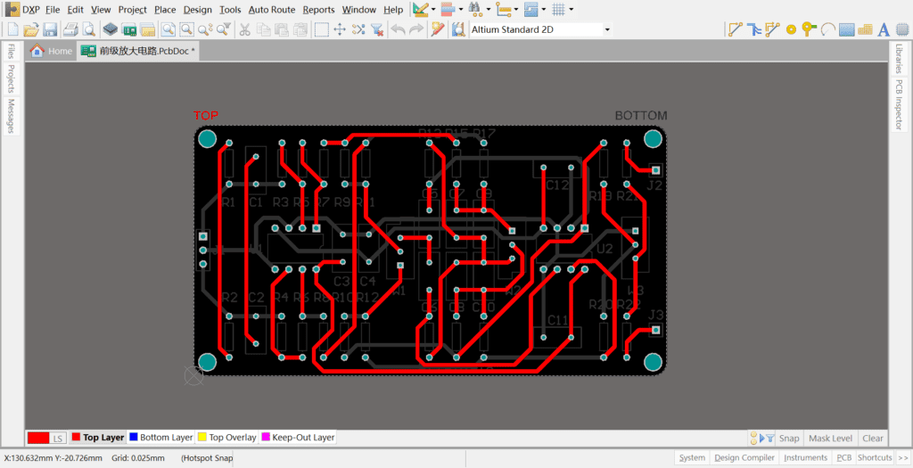
The Highlight Net PCB feature in Altium allows designers to highlight specific nets on the PCB, making it easier to trace connections and identify potential issues. This feature is particularly useful when working with complex designs that may have many different connections and components.
Altium Highlight Net PCB also includes a range of other features that make it easier to design and troubleshoot PCBs. For example, the tool includes a netlist viewer that allows designers to view the connections between components and the different nets on the PCB. Additionally, Altium Highlight Net PCB includes a range of advanced routing features that help designers to optimize the layout of the PCB and ensure that all connections are properly routed.
Overall, Altium Highlight Net PCB is an essential tool for any designer working on complex PCB designs. With its powerful visualization and routing features, this tool makes it easier to design, troubleshoot, and optimize PCBs, ensuring that designs are accurate, reliable, and efficient.
How to Highlight Nets in Altium
Step 1: Open PCB Layout Editor
To highlight nets in Altium, the first step is to open the PCB Layout Editor. Once the editor is open, navigate to the ‘PCB’ tab and select ‘Nets’ from the drop-down menu. This will display a list of all the nets present in the design.
Step 2: Select the Net to Highlight
After opening the Nets tab, select the net that you want to highlight. You can search for a specific net by typing its name in the search bar. Once you have found the net, click on it to select it.
Step 3: Highlight the Net
With the net selected, you can now highlight it. To do this, right-click on the net and select ‘Highlight Net’ from the context menu. The selected net will now be highlighted in a different color, making it easier to distinguish from other nets on the PCB.
In conclusion, highlighting nets in Altium is a simple process that can help you better visualize your design and make it easier to work with. By following these three steps, you can quickly and easily highlight any net in your design.
Benefits of Using Altium Highlight Net PCB

Saves Time and Effort
Altium Highlight Net PCB is a powerful tool that can help designers save a lot of time and effort. With this tool, designers can easily highlight all the nets on the PCB, making it easier to identify and locate specific components. This feature is particularly useful when working on complex designs that involve a large number of components and nets.
In addition, Altium Highlight Net PCB can help designers quickly identify and fix errors in the design. By highlighting all the nets on the PCB, designers can easily spot any issues or errors that may have been missed during the design process. This can save a lot of time and effort, as designers can quickly identify and fix any issues before they become more serious problems.
Improves Accuracy and Efficiency
Altium Highlight Net PCB can also help improve the accuracy and efficiency of the design process. By highlighting all the nets on the PCB, designers can ensure that all the components are properly connected and that there are no errors or issues in the design. This can help improve the overall quality of the design and reduce the risk of errors or issues during the manufacturing process.
In addition, Altium Highlight Net PCB can help designers work more efficiently by allowing them to quickly identify and locate specific components and nets on the PCB. This can save a lot of time and effort, as designers can quickly find the components they need and make any necessary changes or adjustments.
Enhances Design Visualization
Altium Highlight Net PCB can also enhance the visualization of the design. By highlighting all the nets on the PCB, designers can get a better understanding of how the components are connected and how the design works as a whole. This can help designers make better decisions and create more effective designs.
In addition, Altium Highlight Net PCB can help designers create more visually appealing designs by allowing them to highlight specific components or areas of the PCB. This can help designers create more attractive and professional-looking designs that are more appealing to clients and customers.
Overall, Altium Highlight Net PCB is a powerful tool that can help designers save time and effort, improve accuracy and efficiency, and enhance the visualization of the design. With its many features and benefits, Altium Highlight Net PCB is a must-have tool for any PCB designer looking to create high-quality, effective designs.
Best Practices for Using Altium Highlight Net PCB
Use Consistent Naming Conventions
When using Altium Highlight Net PCB, it’s important to use consistent naming conventions for your nets. This will help you keep track of which nets are connected to which components, and make it easier to troubleshoot any issues that arise.
Consider using a standard naming convention, such as prefixing each net name with the name of the component it’s connected to. For example, if you have a resistor R1 connected to a capacitor C2, you might name the net between them “R1_C2”. This will help you quickly identify which nets are connected to which components, and make it easier to navigate your design.
Organize Your Design into Logical Blocks
Another best practice for using Altium Highlight Net PCB is to organize your design into logical blocks. This will help you keep track of which components are connected to which nets, and make it easier to troubleshoot any issues that arise.
Consider grouping components together based on their function or location on the board. For example, you might group all of the components related to power management together in one block, and all of the components related to signal processing in another block. This will make it easier to navigate your design and troubleshoot any issues that arise.
Minimize the Number of Nets on Each Sheet
Finally, when using Altium Highlight Net PCB, it’s important to minimize the number of nets on each sheet. This will help you keep track of which nets are connected to which components, and make it easier to troubleshoot any issues that arise.
Consider breaking your design up into multiple sheets, with each sheet containing only a few nets. This will make it easier to navigate your design and troubleshoot any issues that arise. Additionally, consider using hierarchical design techniques to further simplify your design and reduce the number of nets on each sheet.
By following these best practices, you can use Altium Highlight Net PCB with confidence and create high-quality PCB designs.
