PCB design is an essential part of modern electronics. Whether you are an engineer, hobbyist, or student, learning how to design a PCB can be a valuable skill. However, for beginners, it can be overwhelming to know where to start.
In this article, we will cover the basics of beginner PCB design. We will explain what a PCB is, why it is important, and the different stages involved in the design process. We will also provide tips and resources to help you get started on your first PCB design project. By the end of this article, you will have a better understanding of PCB design and the tools and techniques needed to create your own circuit boards.
Basic Concepts
What is PCB Design?
PCB design is the process of creating a printed circuit board (PCB) that connects electronic components using conductive pathways. PCBs are used in many electronic devices, from smartphones to computers to medical equipment. PCB design involves creating a layout of the electronic components on a board, connecting them using conductive pathways, and ensuring that the board meets the necessary electrical and mechanical requirements.
Why is PCB Design Important?
PCB design is an essential part of electronics engineering. It allows engineers to create complex circuits with a high level of precision, reliability, and efficiency. PCBs can be designed to fit into small spaces, provide high-speed signal transmission, and withstand harsh environments. PCB design also plays a critical role in reducing the cost and time required to manufacture electronic devices.
PCB Design Process
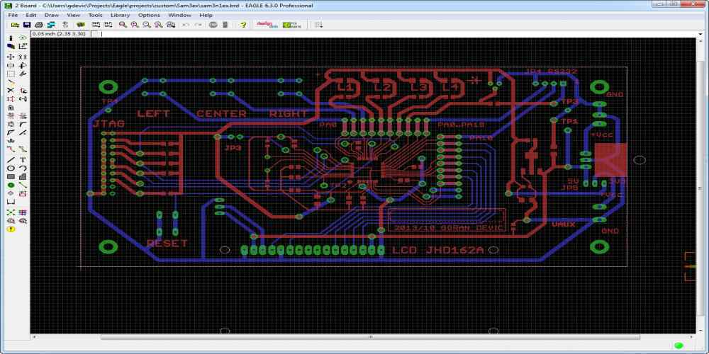
The PCB design process typically involves several stages, including schematic capture, board layout, and manufacturing. In the schematic capture stage, engineers create a diagram of the electronic components and their connections. In the board layout stage, engineers design the physical layout of the PCB, including the placement of components and the routing of conductive pathways. Finally, in the manufacturing stage, the PCB is produced using a variety of techniques, including etching, drilling, and soldering.
In conclusion, PCB design is a critical aspect of electronics engineering, allowing engineers to create complex circuits with precision, reliability, and efficiency. The PCB design process involves several stages, including schematic capture, board layout, and manufacturing. By understanding the basics of PCB design, you can create electronic devices that meet the necessary electrical and mechanical requirements while reducing the cost and time required for manufacturing.
Design Tools

When it comes to designing a PCB, having the right tools is essential. In this section, we will discuss the software and hardware options available for beginners.
Software Options
There are a variety of software options available for designing PCBs. Some popular choices include:
- Eagle PCB Design Software: This software is widely used and offers a free version for beginners.
- KiCAD: This open-source software is free and provides a variety of tools for designing PCBs.
- Altium Designer: This software is known for its user-friendly interface, but it comes with a higher price tag.
Before selecting a software, it’s important to consider your budget, the complexity of your project, and your level of experience.
Hardware Options
In addition to software, there are also hardware options available for designing PCBs. Some popular choices include:
- Breadboards: These are a great option for beginners who want to experiment with circuit designs before moving on to a more permanent solution.
- PCB Prototyping Boards: These boards are designed for prototyping and can be used to create a more permanent solution once the design has been finalized.
- CNC Machines: These machines are used to create PCBs from scratch and are a good option for those who want complete control over the design process.
Again, it’s important to consider your budget, the complexity of your project, and your level of experience when selecting a hardware option.
By selecting the right design tools, beginners can create high-quality PCBs with ease.
Design Guidelines
When designing a printed circuit board (PCB), there are a few guidelines that are important to follow to ensure proper functionality and reliability. These guidelines include component placement, trace routing, and power and ground planes.
Component Placement
Proper component placement is crucial for a successful PCB design. Components should be placed in a way that minimizes the length of traces and reduces the possibility of interference. It is also important to consider the orientation of polarized components, such as capacitors and diodes.
To aid in component placement, it is helpful to use a software tool that allows for 3D visualization of the PCB. This can help identify potential issues with component placement and ensure that components fit properly within the designated space.
Trace Routing
Trace routing involves the placement of conductive pathways on the PCB. It is important to keep traces as short as possible and avoid crossing over each other to reduce the likelihood of interference. Traces should also be wide enough to handle the required current without overheating.
When routing traces, it is important to avoid acute angles and use gradual turns instead. This helps to minimize the possibility of electromagnetic interference and ensures that the signal remains clear.
Power and Ground Planes
Power and ground planes are essential for proper functioning of the PCB. The power plane provides a stable voltage source, while the ground plane serves as a reference point for the circuit. These planes should be as large as possible to minimize resistance and provide adequate current carrying capacity.
When designing the power and ground planes, it is important to ensure that they are connected properly to all components. This can be achieved through the use of vias, which allow for the connection of components on different layers of the PCB.
By following these design guidelines, a beginner can create a functional and reliable PCB.
Design Verification
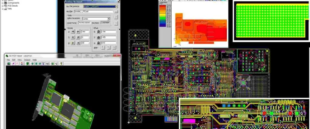
Before sending your PCB design to fabrication, it’s important to verify that it meets certain design requirements. This process is known as design verification. There are two main aspects of design verification: Design Rule Check and Signal Integrity Analysis.
Design Rule Check
Design Rule Check (DRC) is a process that checks your PCB design against a set of predefined design rules. These rules ensure that your design meets certain manufacturing requirements and that it can be fabricated correctly. DRC checks for issues such as minimum trace width and spacing, via size and placement, and clearance between components.
Most PCB design software includes a DRC tool that automatically checks your design for rule violations. It’s important to run a DRC before sending your design to fabrication to avoid costly errors and delays.
Signal Integrity Analysis
Signal Integrity Analysis (SIA) is a process that checks your PCB design for potential signal integrity issues. This includes checking for reflections, crosstalk, and other issues that can affect signal quality. SIA is especially important for high-speed designs, where even small signal integrity issues can cause significant problems.
Most PCB design software includes an SIA tool that can simulate signal behavior and identify potential issues. It’s important to run an SIA before sending your design to fabrication to ensure signal quality and avoid issues in the final product.
In summary, design verification is an important step in the PCB design process. By running a DRC and SIA, you can ensure that your design meets manufacturing requirements and has good signal integrity.
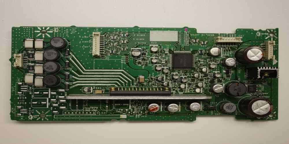
Manufacturing Considerations
When designing a PCB, it is important to keep in mind the manufacturing considerations to ensure that the PCB can be manufactured without any issues. There are two main aspects to consider when it comes to manufacturing: Design for Assembly and Design for Test.
Design for Assembly
Design for Assembly (DFA) is a set of guidelines that aim to make the assembly process of a PCB as efficient as possible. By following these guidelines, the assembly process can be streamlined, which can reduce the overall cost of manufacturing. Some of the guidelines to consider when designing for assembly include:
- Minimizing the number of components
- Using standardized components
- Avoiding the use of through-hole components
- Ensuring that components are placed in a logical and organized manner
- Minimizing the number of solder joints
- Using surface mount technology (SMT)
By following these guidelines, the assembly process can be made much more efficient, which can ultimately lead to a better end product.
Design for Test
Design for Test (DFT) is another set of guidelines that aim to make the testing process of a PCB as efficient as possible. By following these guidelines, the testing process can be streamlined, which can reduce the overall cost of manufacturing. Some of the guidelines to consider when designing for test include:
- Including test points on the PCB
- Using self-test features
- Minimizing the number of test points
- Ensuring that test points are easily accessible
By following these guidelines, the testing process can be made much more efficient, which can ultimately lead to a better end product.
In conclusion, by considering the manufacturing aspects of a PCB design, the assembly and testing process can be made much more efficient, which can ultimately lead to a better end product. By following the guidelines of Design for Assembly and Design for Test, the PCB can be manufactured with ease and tested with confidence.
Conclusion
In this article, we have covered the basics of PCB design for beginners. We have discussed the importance of understanding the design process, selecting the right software tools, and following good design practices.
We have also covered the key components of a PCB, including the substrate, copper layers, vias, and pads. We have discussed how to create a schematic diagram, how to lay out components on a PCB, and how to route the traces between them.
One of the most important things to remember when designing a PCB is to keep it simple. Avoid unnecessary complexity, and focus on creating a clean, well-organized design that is easy to manufacture and test.
In addition, it is important to be patient and persistent when designing a PCB. Don’t be afraid to experiment and try new things, but also don’t be discouraged if things don’t work out the first time. With practice and experience, you will become a skilled PCB designer.
Finally, remember that there is always more to learn about PCB design. Keep reading, exploring, and experimenting, and you will continue to improve your skills and knowledge over time.
