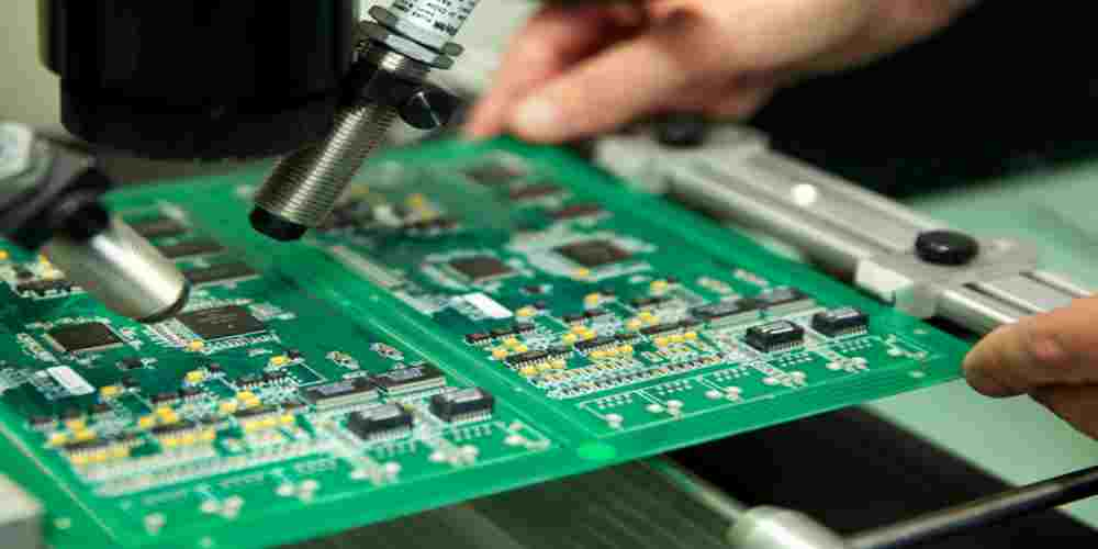
Amplifier driver PCB layout is an essential aspect of designing high-performance audio amplifiers. The PCB layout plays a crucial role in determining the overall performance of the amplifier. It is responsible for ensuring that the signal is transmitted effectively from the input to the output without any distortion or noise.
The layout of the PCB determines the physical placement of the components, including the resistors, capacitors, and transistors. The placement of these components can have a significant impact on the performance of the amplifier. The layout must be designed in a way that minimizes the length of the signal path and reduces the chances of interference from other components. Additionally, the layout must be optimized to reduce noise and distortion, which can negatively impact the sound quality of the amplifier.
Basics of Amplifier Driver PCB Layout
Grounding
Grounding is an essential aspect of amplifier driver PCB layout. A solid ground plane is necessary to minimize noise and interference. It is important to keep the ground plane as large as possible and connect it to the chassis ground. Grounding of the input, output, and power supply sections should be separated to avoid ground loops. It is also important to keep the ground traces as short as possible.
Power Supply Decoupling
Power supply decoupling is important to ensure stable operation of the amplifier driver circuit. Decoupling capacitors should be placed as close as possible to the power supply pins of the IC. The value of the decoupling capacitors should be selected based on the frequency range of the circuit. A combination of electrolytic and ceramic capacitors can be used to provide low and high-frequency decoupling.
Signal Traces
Signal traces should be kept as short as possible to minimize noise and interference. The input and output traces should be routed away from the power supply traces to avoid coupling. The traces should be routed in a way that minimizes crosstalk between channels. It is also important to keep the traces as wide as possible to minimize resistance and inductance.
Component Placement
Component placement is crucial to ensure proper operation of the amplifier driver circuit. The IC should be placed as close as possible to the decoupling capacitors. The input and output connectors should be placed away from the power supply section to avoid coupling. The components should be placed in a way that minimizes the length of the traces. It is also important to keep the components away from the edges of the PCB to avoid interference.
In summary, proper grounding, power supply decoupling, signal trace routing, and component placement are essential for a successful amplifier driver PCB layout.
Considerations for High-Frequency Applications

RF Filtering
In high-frequency applications, it is essential to have a clean power supply. The power supply should be filtered to remove any noise and ripple. A simple RC filter can be used to filter the power supply. The values of the resistor and capacitor should be chosen to achieve the desired cutoff frequency.
It is also important to filter the input and output signals. A low-pass filter can be used to filter the input signal, and a high-pass filter can be used to filter the output signal. The values of the components should be chosen to achieve the desired cutoff frequency.
Transmission Line Effects
In high-frequency applications, the PCB traces act as transmission lines. The characteristic impedance of the transmission line should match the impedance of the source and load. This will minimize reflections and maximize power transfer.
It is also important to minimize the length of the traces. The longer the trace, the more it will act as an antenna and pick up noise. The traces should be kept as short as possible.
EMI Shielding
In high-frequency applications, electromagnetic interference (EMI) can be a problem. EMI can be caused by the amplifier driver itself or by external sources.
To minimize EMI, the amplifier driver should be shielded. The shield should be connected to ground and should completely surround the amplifier driver. The shield should also be connected to the PCB ground plane.
External sources of EMI can be minimized by using twisted pair cables and by keeping the cables as short as possible.
Overall, when designing a PCB layout for high-frequency applications, it is important to consider RF filtering, transmission line effects, and EMI shielding. By taking these factors into account, the amplifier driver can operate at its full potential without interference.
| RF Filtering | Transmission Line Effects | EMI Shielding |
|---|---|---|
| Clean power supply | Match characteristic impedance | Shield amplifier driver |
| Filter input and output signals | Keep traces as short as possible | Connect shield to ground |
| Use low-pass and high-pass filters | Use twisted pair cables |
Thermal Management
Heat Sinks
Heat sinks are an essential component of thermal management in amplifier driver PCB layouts. They are used to dissipate heat from power transistors, which can generate a lot of heat during operation. Heat sinks come in various shapes and sizes, and their effectiveness depends on their surface area and the airflow around them.
When selecting a heat sink, it’s important to consider the power dissipation of the transistors and the maximum temperature that they can withstand. A heat sink that is too small or ineffective can cause the transistors to overheat, leading to reduced performance and potentially damaging the components.
Thermal Pads
Thermal pads are used to improve the thermal contact between the heat sink and the power transistors. They are made of a soft material that conforms to the shape of the components and fills any gaps between them. This improves the heat transfer between the components and the heat sink, ensuring that the heat is dissipated effectively.
When selecting a thermal pad, it’s important to choose a material that has good thermal conductivity and can withstand high temperatures. The thickness of the pad should also be chosen carefully to ensure that it provides good contact between the components and the heat sink.
Copper Pour
Copper pour is a technique used in PCB layout to improve thermal management. It involves filling empty spaces on the PCB with copper to create a large thermal mass. This helps to dissipate heat from the components and improve the overall thermal performance of the circuit.
When using copper pour, it’s important to ensure that the copper is connected to a ground plane to avoid creating unwanted electrical noise. The size and shape of the copper pour should also be carefully chosen to ensure that it provides the desired thermal performance.
In conclusion, thermal management is an important consideration in amplifier driver PCB layouts. Heat sinks, thermal pads, and copper pour are all effective techniques for dissipating heat and improving the overall thermal performance of the circuit. By carefully selecting and implementing these techniques, it’s possible to ensure that the amplifier driver operates at optimal performance and reliability.
Advanced Techniques
Mixed-Signal Layout
Mixed-signal circuits require careful layout to minimize noise and crosstalk. To achieve good performance, it is important to separate analog and digital signals and keep them away from each other. This can be done by using separate ground planes and power supplies for each section. Additionally, it is important to use proper decoupling capacitors to reduce noise and to place them as close as possible to the ICs.
Impedance Matching
Impedance matching is crucial for high-frequency circuits to ensure maximum power transfer. A good practice is to use transmission lines with controlled impedance to match the output of the driver to the input of the amplifier. A popular technique is to use a microstrip line, which is a type of transmission line with a thin strip of metal on top of a grounded substrate. It is important to calculate the correct trace width and thickness to achieve the desired impedance.
Power Integrity Analysis
Power integrity analysis is necessary to ensure that the power supply voltage remains stable and free of noise. This is especially important for high-frequency circuits, where small variations in voltage can cause significant performance degradation. A good practice is to use a power plane with multiple vias to reduce the inductance and resistance of the power supply. Additionally, it is important to use proper decoupling capacitors to filter out high-frequency noise.
In conclusion, advanced techniques such as mixed-signal layout, impedance matching, and power integrity analysis are crucial for designing high-performance amplifier driver PCB layouts. By following these best practices, designers can minimize noise and crosstalk, ensure maximum power transfer, and maintain stable power supply voltage.
Conclusion
In conclusion, the PCB layout of an amplifier driver is a critical aspect that should not be overlooked. A well-designed PCB layout can significantly improve the overall performance of the amplifier driver.
To achieve a good PCB layout, it is essential to follow some best practices, such as keeping the signal traces as short as possible, minimizing the loop area, and ensuring proper grounding. Additionally, the use of high-quality components and careful placement of components can also improve the performance of the amplifier driver.
When designing a PCB layout, it is crucial to consider the specific requirements of the amplifier driver and the intended application. For example, if the amplifier driver is intended for high-frequency applications, it is essential to pay close attention to the parasitic capacitance and inductance of the PCB traces and components.
Overall, the PCB layout of an amplifier driver is a complex and challenging task that requires careful planning, attention to detail, and extensive knowledge of electronics. By following best practices and taking the time to design a high-quality PCB layout, you can ensure that your amplifier driver performs at its best and delivers excellent results.
