Circuit board layout design is an essential aspect of electronic product development. It involves the arrangement of electronic components on a printed circuit board (PCB) to ensure optimal performance and functionality of the device. The layout design of a circuit board can affect the overall performance, reliability, and cost of the final product.
The process of circuit board layout design requires careful consideration of various factors, including the size and shape of the board, the number and type of components, and the electrical and mechanical requirements of the device. The design must also take into account the manufacturing process, as well as any regulations and standards that apply to the product.
With the increasing demand for smaller, lighter, and more complex electronic devices, the importance of circuit board layout design has grown significantly. A well-designed circuit board can help to reduce costs, improve performance, and enhance the overall user experience of the product. As such, it is crucial for electronics engineers and designers to have a solid understanding of circuit board layout design principles and techniques.
Basics of Circuit Board Layout Design
Components Placement
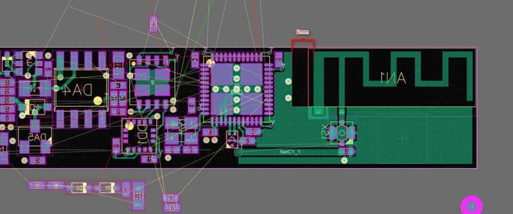
The first step in circuit board layout design is component placement. The placement of components on the board is critical to the overall performance of the circuit. Components should be placed in a way that minimizes the length of the traces between them, which reduces the overall resistance and capacitance of the circuit.
When placing components, it is important to consider the size and shape of the board, as well as the location of power and ground connections. Components should be placed in a way that allows for efficient routing of traces and minimizes the risk of signal interference.
Routing and Traces
Routing and traces refer to the paths that signals take through the circuit board. The routing of traces is critical to the overall performance of the circuit. Traces should be kept as short as possible, and the width of the traces should be appropriate for the amount of current that they will carry.
When routing traces, it is important to avoid crossing over other traces and to minimize the amount of bends in the trace. This reduces the risk of signal interference and helps to ensure that the circuit operates as intended.
Signal Integrity
Signal integrity refers to the ability of a circuit to transmit signals without distortion or interference. This is critical to the overall performance of the circuit. To ensure signal integrity, it is important to minimize the length of the traces, reduce the number of vias, and avoid crossing over other traces.
Other factors that can affect signal integrity include the type of components used, the quality of the solder joints, and the overall quality of the circuit board itself. By paying close attention to these factors, it is possible to design a circuit board that delivers excellent signal integrity and reliable performance.
Design Considerations

When designing a circuit board layout, there are several factors to consider to ensure the board functions properly. Three of the most important considerations are the power distribution network, thermal management, and EMI/EMC compliance.
Power Distribution Network
The power distribution network (PDN) is responsible for ensuring that power is distributed evenly throughout the board. This is important because uneven power distribution can cause voltage drops and other issues that can impact the board’s performance. To ensure proper PDN design, consider the following:
- Use multiple power planes to distribute power evenly
- Place decoupling capacitors near the power pins of each component
- Use low-ESR (Equivalent Series Resistance) capacitors for decoupling
- Use wider traces for power distribution to minimize resistance
Thermal Management
Thermal management is important to prevent components from overheating, which can cause damage to the board and impact its performance. To ensure proper thermal management, consider the following:
- Place components in areas with good airflow
- Use thermal vias to transfer heat away from components
- Use heat sinks on components that generate a lot of heat
- Use a thermal analysis tool to simulate and optimize heat dissipation
EMI/EMC Compliance
EMI (Electromagnetic Interference) and EMC (Electromagnetic Compatibility) compliance is important to ensure that the board does not interfere with other electronic devices or vice versa. To ensure proper EMI/EMC compliance, consider the following:
- Use a ground plane to reduce EMI emissions
- Place sensitive components away from high-speed signals and power lines
- Use shielding to reduce EMI emissions and susceptibility
- Use filters to reduce EMI emissions and susceptibility
By considering these design considerations, you can ensure that your circuit board layout functions properly and meets the necessary requirements for your application.
Advanced Techniques
High-Speed Design
When designing a high-speed circuit board, it is important to consider signal integrity and timing. Here are some advanced techniques to ensure your high-speed design works as intended:
- Use controlled impedance routing to minimize reflections and signal distortion.
- Place decoupling capacitors close to power and ground pins to reduce noise and voltage fluctuations.
- Use differential pairs for high-speed signals to improve noise immunity and reduce crosstalk.
- Minimize the number of vias and keep them away from high-speed signals to reduce signal reflections and losses.
- Use length matching to ensure that signals arrive at the same time and reduce skew.
Mixed-Signal Design
Mixed-signal design involves the integration of analog and digital circuits on the same board. Here are some advanced techniques to ensure your mixed-signal design works as intended:
- Separate analog and digital ground planes to minimize noise coupling and reduce interference.
- Use guard traces to protect sensitive analog signals from noise and interference.
- Place analog and digital components on opposite sides of the board to reduce interference.
- Use filters and shielding to reduce noise and improve signal quality.
- Use low-dropout regulators (LDOs) for analog power to reduce noise and voltage fluctuations.
RF Design
RF design involves the design of circuits that operate at high frequencies. Here are some advanced techniques to ensure your RF design works as intended:
- Use microstrip or stripline transmission lines to minimize signal loss and reduce interference.
- Use impedance matching to ensure maximum power transfer and reduce signal reflections.
- Use filters and shielding to reduce noise and improve signal quality.
- Use low-noise amplifiers (LNAs) to amplify weak RF signals and improve sensitivity.
- Use directional couplers to measure RF power and signal strength.
Remember, these are just a few advanced techniques for circuit board layout design. Always consult industry standards and best practices to ensure your design meets the necessary requirements.
Tools and Software

CAD Tools
CAD (Computer-Aided Design) tools are essential for creating circuit board layout designs. They allow designers to create and modify schematics, layout components, and route traces. Some of the popular CAD tools for circuit board layout design are Altium Designer, Eagle PCB, KiCAD, and OrCAD PCB Designer.
Altium Designer is a comprehensive CAD tool that includes schematic capture, PCB layout, and design verification features. Eagle PCB is a powerful and easy-to-use CAD tool that is popular among hobbyists and professionals alike. KiCAD is a free and open-source CAD tool that offers a suite of tools for schematic capture, PCB layout, and 3D visualization. OrCAD PCB Designer is a professional-grade CAD tool that includes advanced features like signal integrity analysis, design rule checking, and autorouting.
Simulation Software
Simulation software is used to simulate the behavior of a circuit board design before it is built. This allows designers to identify and fix potential issues before the board is manufactured. Some of the popular simulation software for circuit board layout design are LTSpice, PSpice, and Proteus.
LTSpice is a free and easy-to-use simulation software that allows designers to simulate analog circuits. PSpice is a professional-grade simulation software that includes advanced features like mixed-signal simulation and Monte Carlo analysis. Proteus is a comprehensive simulation software that includes schematic capture, PCB layout, and simulation features.
Design for Manufacturing Tools
Design for Manufacturing (DFM) tools are used to ensure that a circuit board design can be manufactured efficiently and cost-effectively. They analyze the design for potential manufacturing issues and provide suggestions for improving the design. Some of the popular DFM tools for circuit board layout design are Valor NPI, CAM350, and GerbTool.
Valor NPI is a DFM tool that includes features like panelization, stencil design, and design rule checking. CAM350 is a comprehensive DFM tool that includes features like design verification, panelization, and fabrication output. GerbTool is a DFM tool that includes features like design rule checking, panelization, and fabrication output.
In conclusion, CAD tools, simulation software, and DFM tools are essential for circuit board layout design. They allow designers to create and modify designs, simulate the behavior of the design, and ensure that the design can be manufactured efficiently and cost-effectively.
